
Melt Planarization Of Solar Cell Bus Bars

Inactive Publication Date: 2010-05-27
PALO ALTO RES CENT INC
View PDF99 Cites 5 Cited by
  • Summary
  • Abstract
  • Description
  • Claims
  • Application Information

AI Technical Summary

Benefits of technology

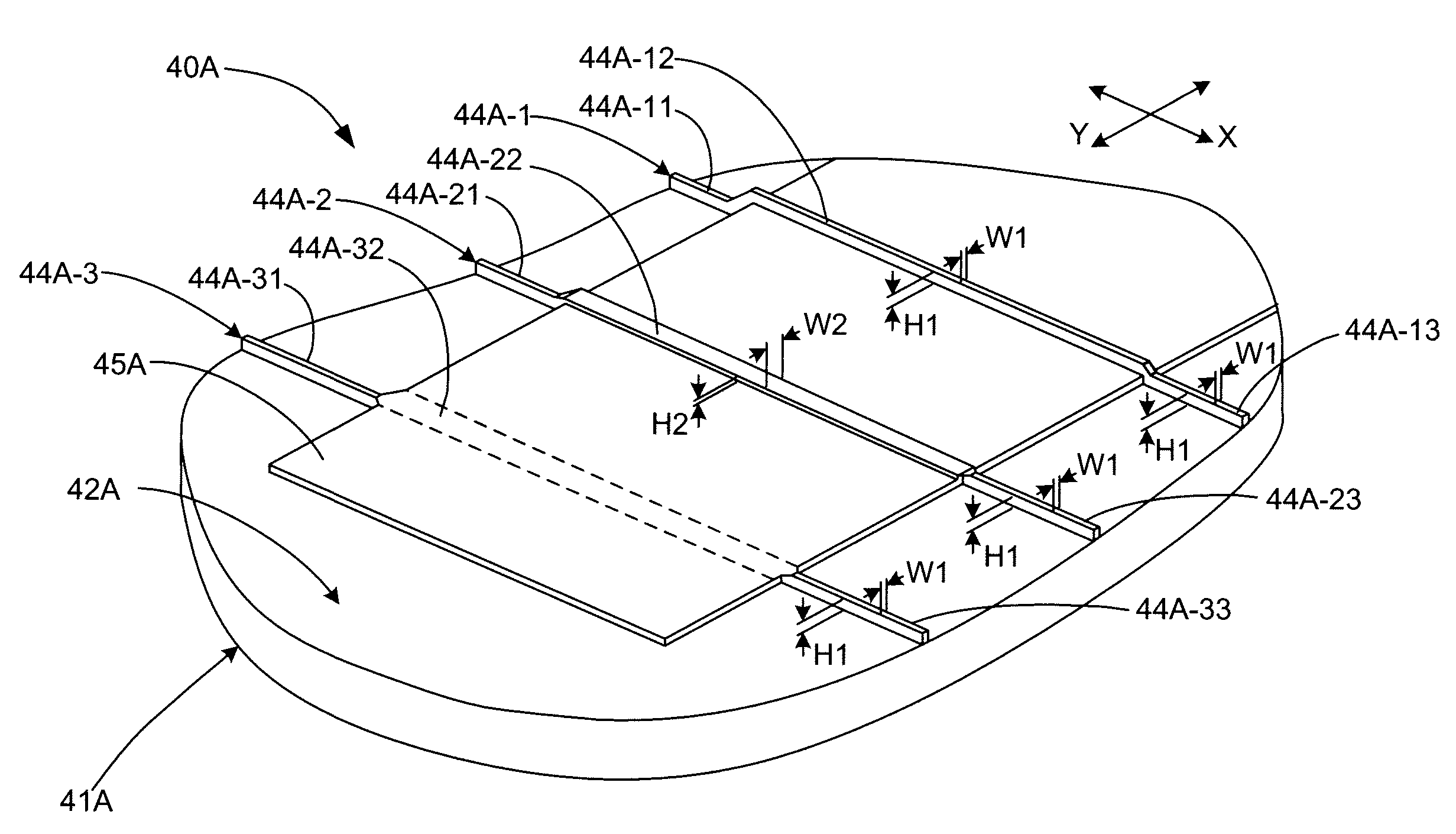
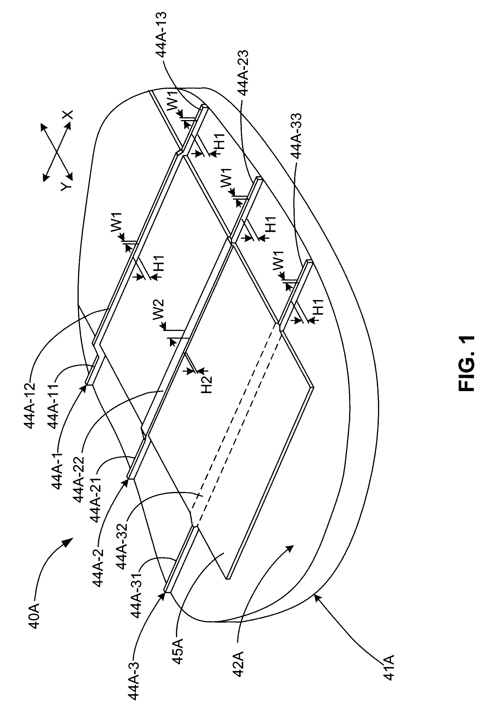
[0007]The present invention is directed to solar cells (and other electric electronic and devices) having bus bars and high aspect-ratio gridlines printed on a substrate, wherein localized melting is performed to slump or flatten the gridline “vertex” portions that are disposed on the bus bars, while maintaining the high aspect-ratio of gridlines portions disposed on the substrate between the bus bars. The localized melting thus planarizes the bus bars in order to facilitate reliable connection of metal ribbon (string metallization) without additional processing, thereby avoiding the peaked topography problem associated with the prior art. In addition, critical portions of the metallization structure, namely the gridlines, can remain in the form of highly conductive elemental metals. Further, no mechanical treatment for the fragile wafers is needed, and in some embodiments standard processing techniques can be utilized, thereby minimizing production costs.
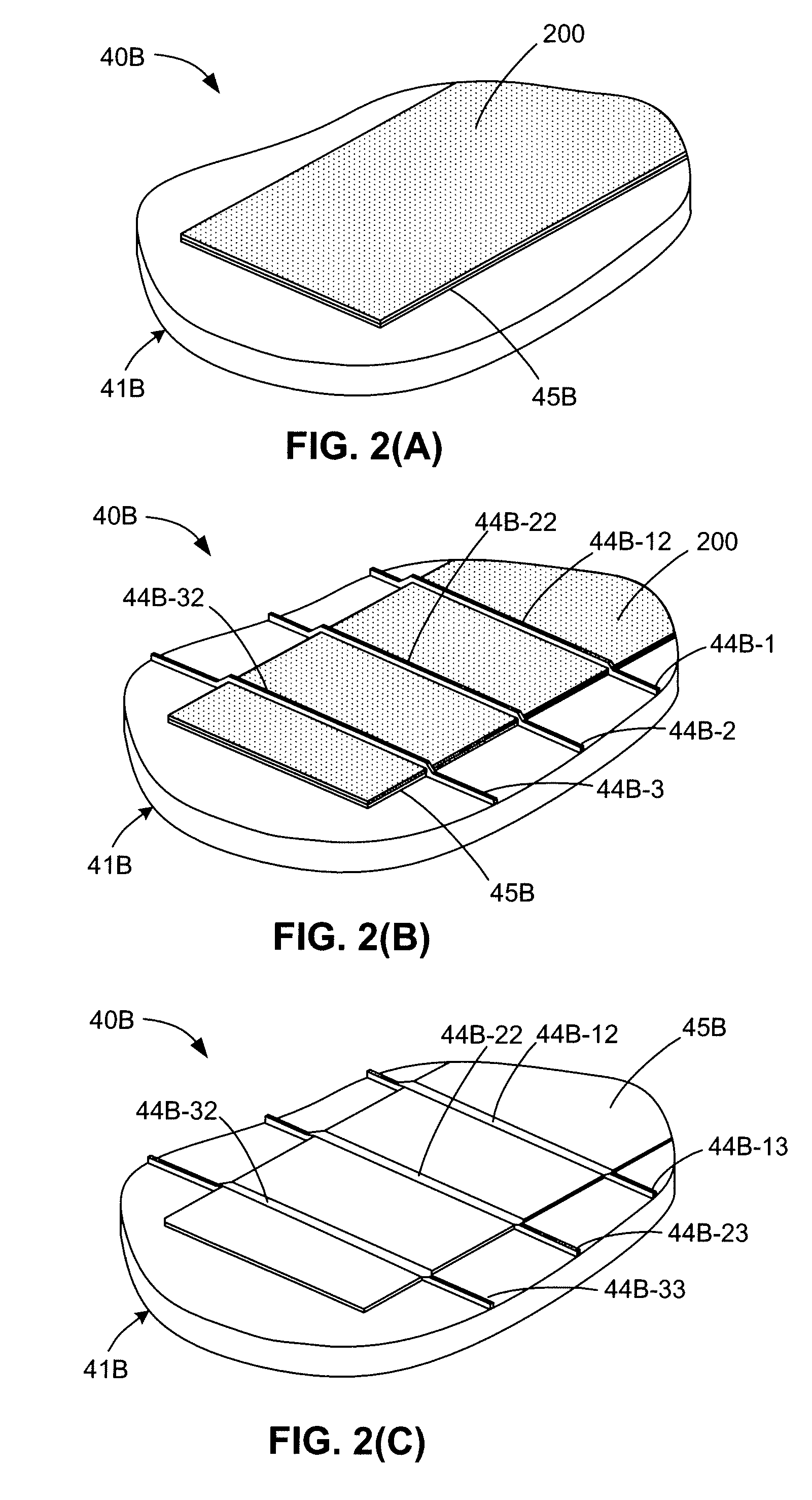
[0009]According to another embodiment of the present invention, a method for producing solar cells includes disposing (e.g., printing, depositing, stamping, or spraying) a first ink to form elongated bus bars on a substrate, printing a second ink to form parallel elongated gridlines that are orthogonal to and overlap the bus bars, and then inducing localized melting of portions of the gridlines that overlap the bus bars without altering the cross-section of portions of the gridlines that is disposed on the substrate. In one embodiment, the printing process is performed by extrusion printing bus bar material (first ink) onto the substrate such that the bus bar material forms elongated, relatively low aspect ratio parallel bus bars in a first (Y-axis) direction, and then turning the printhead (or substrate) and printing the gridline material (second ink) such that the gridline material forms elongated, relatively high aspect ratio parallel gridlines. Each of the elongated gridlines is printed such that it includes lower (first) gridline portions that are formed directly on the substrate surface, and elevated (second) gridline portions that extend between corresponding lower gridline portions and are supported by an associated bus bar. When initially printed, both the lower and elevated gridline portions have an initial cross-section including a first aspect ratio. According to an aspect of the invention, the localized melting process is performed such that the elevated gridline portion slumps (i.e., assumes a melted cross-section having a lower (second) aspect ratio), but the lower gridline portions retain the initial cross-section (i.e., maintain the initial aspect ratio) cross-section.

Problems solved by technology

However, the resulting structure is not necessarily optimal from a cell performance perspective however because the relatively low aspect ratio causes gridlines 44 to generate an undesirably large shadowed surface area (i.e., gridlines 44 prevent a significant amount of sunlight from passing through a large area of upper surface 22 into substrate 21, as depicted in FIG. 18 by light beam L2), which reduces the ability of solar cell 20 to generate electricity.
However, simply reducing the width of gridlines 44 (i.e., without increasing the gridlines' cross-sectional area by increasing their height dimension) could undesirably limit the current transmitted to the applied load, and forming high aspect ratio gridlines using screen printing techniques would significantly increase production costs.
Although extrusion printing provides advantages over screen printing (e.g., higher aspect ratio gridlines), these advantages are partially offset by the peaked topography of each vertex 44-1B, i.e., where each gridline 44-1 crosses bus bar 45-1, which can make soldering the stringing metallization (i.e., the metal ribbon) difficult or unreliable.
However, in the case of coextrusion printing, the present inventors have observed that, during the subsequent required firing process, if the gridline material resides beneath the bus bar, the bus bar metal tends to float and separate from the gridlines, causing an open circuit.
Furthermore, the bus bar would still have an undulating surface which still might decrease the reliability of the soldered connection.
There is a characteristic shrinkage and densification of the metallization ink, however, the ink does not at any point become liquid which would enable it to flow, as this would cause the metal to ball up on the substrate causing breaks.
For this reason, one can not simply planarize the metallization on the bus bars by briefly melting it, as it would damage the device.

Method used


Image

  • Melt Planarization Of Solar Cell Bus Bars
  • Melt Planarization Of Solar Cell Bus Bars
  • Melt Planarization Of Solar Cell Bus Bars

Examples


Embodiment Construction

[0027]The present invention relates to an improvement in micro-extrusion systems. The following description is presented to enable one of ordinary skill in the art to make and use the invention as provided in the context of a particular application and its requirements. As used herein, directional terms such as “upper”, “top”, “lower”, “bottom”, “front”, “rear”, and “lateral” are intended to provide relative positions for purposes of description, and are not intended to designate an absolute frame of reference. Various modifications to the preferred embodiment will be apparent to those with skill in the art, and the general principles defined herein may be applied to other embodiments. Therefore, the present invention is not intended to be limited to the particular embodiments shown and described, but is to be accorded the widest scope consistent with the principles and novel features herein disclosed.

[0028]FIG. 1 is a simplified perspective diagram showing a portion of a front side...


PUM


Abstract

Solar cells include bus bars and high aspect-ratio gridlines that are printed on a substrate, and localized melting is induced to slump or flatten the gridline “vertex” portions that are disposed on the bus bars, while maintaining the high aspect-ratio of gridlines portions disposed on the substrate between the bus bars. The localized melting process is induced using one of several disclosed methods, such as rheological melting in which the two printed inks produce a compound that is relatively liquid. Localized melting is also induced using a deliquescing material (e.g., a flux or a solvent film) that is applied to the bus bar or gridline material. Also, eutectic melting is induced using a processing temperature that is between a melting point of the combined gridline / bus bar inks and the individual melting points of the inks alone. Laser-based melting and the use of copolymers is also disclosed.

Description

FIELD OF THE INVENTION[0001]The present invention is related to integrated circuit (IC) devices, and more particularly to IC devices that include bus bars, such as solar cells.BACKGROUND[0002]FIG. 9 is a simplified diagram showing an exemplary conventional solar cell 40 formed on a semiconductor substrate 41 that converts sunlight into electricity by the inner photoelectric effect. Solar cell 40 is formed on a semiconductor substrate 41 that is processed using known techniques to include an n-type doped upper region 41A and a p-type doped lower region 41B such that a pn-junction is formed near the center of substrate 41. Disposed on an upper surface 42 of semiconductor substrate 41 are a series of parallel metal gridlines (fingers) 44 (shown in end view) that are electrically connected to n-type region 41A. A substantially solid conductive layer 46 is formed on a lower surface 43 of substrate 41, and is electrically connected to p-type region 41B. An antireflection coating 47 is typ...

Claims


Application Information

Patent Timeline
IPC IPC(8): H01L31/0216H01L31/18
CPCY02E10/50H01L31/022425
Inventor FORK, DAVID K.KALIO, ANDRERAO, RANJEET
Owner PALO ALTO RES CENT INC
Learn More