Wiring board, semiconductor device and semiconductor element

a technology of wiring patterns and semiconductor elements, applied in the field of wiring patterns, can solve the problems of difficult to satisfy this requirement, limited number of wiring patterns capable of being formed between the loading pads, and the semiconductor device, and achieve the effect of preventing voltage changes and easy charging

Active Publication Date: 2010-05-27
SHINKO ELECTRIC IND CO LTD
View PDF3 Cites 7 Cited by
  • Summary
  • Abstract
  • Description
  • Claims
  • Application Information

AI Technical Summary

Benefits of technology

[0047]In this way, on the entire face of the other side of the wiring board having a wider area than that of the semiconductor element to be loaded, the necessary number of external connecting terminal pads can be formed. Thus, limitation of the number of the external connecting terminals which can be formed on the wiring board can be cancelled and the pitch between the external connecting terminals can be easily charged.
[0048]In addition, in this invention, the loading pads constituting the area pads of the wiring board are electrically connected to the external connecting terminal pads formed in a lattice pattern in the central region of the other side of the wiring board and its vicinity through the nearest area pad vias passing through the wiring board encircled by the external connecting terminal pads and the wiring patterns; and further the plurality of loading pads constituting the area pads commonly use one of the area pad vias. Thus, the connecting distance between the loading pads constituting the area pads and the corresponding external connecting terminal pads can be shortened to the utmost so that when the loading pads are used as the power supply pads, changes in a voltage can be prevented.

Problems solved by technology

However, the pitch between the loading pads corresponding to the electrode terminals 202, 202, of the semiconductor element 200 is so narrow that the number of the wiring patterns capable of being formed between the loading pads is limited.
However, it is very difficult to satisfy this requirement in the semiconductor device shown in FIG. 11 because the pitch between the electrode terminals 202, 202, of the semiconductor element 200 must be first changed.

Method used


Image

  • Wiring board, semiconductor device and semiconductor element
  • Wiring board, semiconductor device and semiconductor element
  • Wiring board, semiconductor device and semiconductor element

Examples


Embodiment Construction

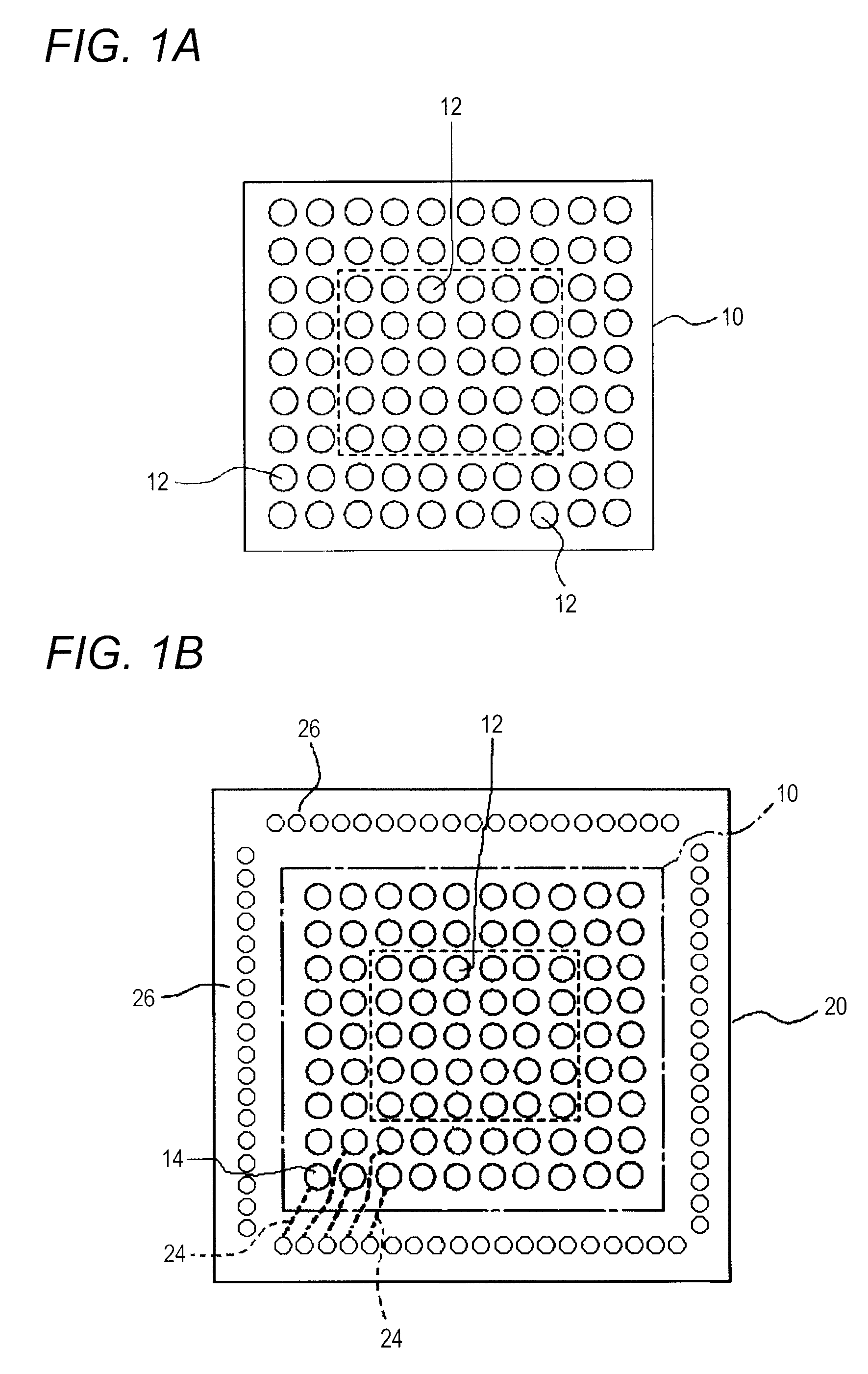
[0061]An example of a semiconductor element to be loaded on a wiring board according to this invention is shown in FIG. 1A. In the semiconductor element 10 shown in FIG. 1A, electrode terminals 12, 12, . . . are formed on the entire surface of its one side. Of these electrode terminals 12, 12, . . . , the electrode terminals 12, 12 formed in the central region encircled by a dotted line and its vicinity are mainly those for power supply and for grounding.

[0062]Further, the electrode terminals 12, formed in two rows on the edge side of the semiconductor element 10 (outside the dotted line) are mainly those for signals.

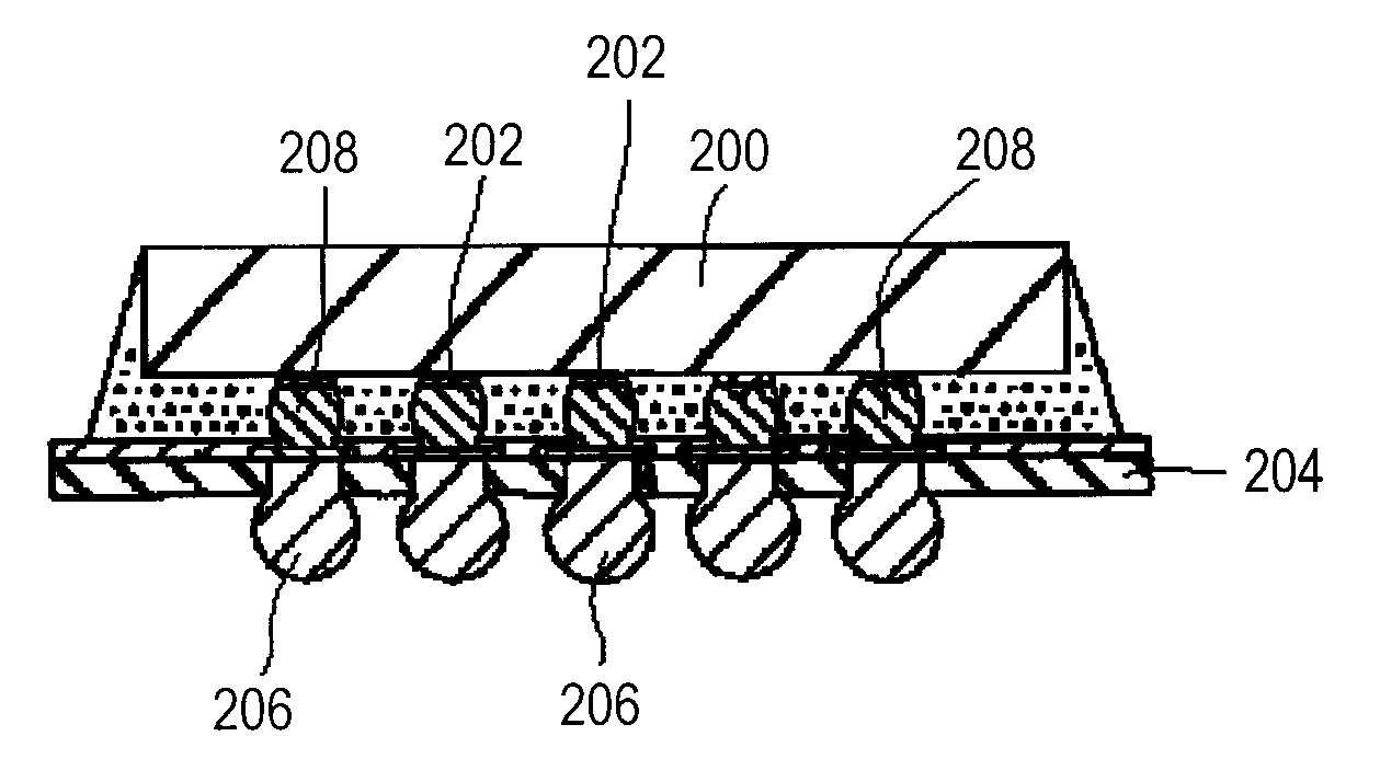
[0063]The wiring board 20 shown in FIG. 1B on which the above semiconductor element 10 is loaded is formed of a resin board of a single layer. A semiconductor element loading face is formed on the one side of the wiring board 20, and as seen form FIG. 1B, it has a wider area than that of the semiconductor element 10. On the semiconductor element loading face, formed are...


PUM


Abstract

On a semiconductor element loading face, wiring patterns are drawn out from those formed in the vicinity of the edge of the semiconductor element of the loading pads formed to correspond to the electrode terminals of the semiconductor element, and connected to via pads formed in the vicinity of the edge of the semiconductor element loading face; area pads constructed of the loading pads corresponding to the electrode terminals formed in the central region of the semiconductor element and its vicinity are electrically connected to external connecting terminal pads formed in the central region on the other side of the wiring board and its vicinity, through the nearest area pad vias encircled by the external connecting terminal pads and passing through the wiring board and the wiring patterns; and a plurality of the loading pads constituting the area pads commonly use one of the area pad vias.

Description

CROSS-REFERENCE TO RELATED APPLICATION[0001]This application is based on and claims priority under 35 U.S.C. §119 from Japanese Patent Application No. 2008-299052 filed on Nov. 25, 2008.BACKGROUND OF THE INVENTION[0002]1. Technical Field[0003]This invention relates to a wiring board, a semiconductor device and a semiconductor element, and more particularly to a wiring board on which a semiconductor element with electrode terminals on the entire face of the one side thereof is loaded, a semiconductor device with the semiconductor element loaded on the wiring board, and a semiconductor element loaded on the wiring board.[0004]2. Related Art[0005]On the one side of a wiring board 100 with a conventional semiconductor element 102 loaded thereon as shown in FIG. 12A, formed is a semiconductor element loading face having a wider area than that of the semiconductor element 102 to be loaded. On the semiconductor element loading face, pads 104, 104, . . . are formed which are to be connected...

Claims


Application Information

Patent Timeline
Patent Type & Authority Applications(United States)
IPC IPC(8): H01L23/488H01R12/06H01R12/51
CPCH01L23/49838H01L24/16H01L24/17H01L2224/16H05K2201/10674H05K1/113H05K1/114H05K2201/09627H01L2924/15311H01L2224/0554H01L2224/05568H01L2224/05573H01L2924/00014H01L2224/05599H01L2224/0555H01L2224/0556
Inventor OZAWA, TAKASHISATO, HITOSHI
Owner SHINKO ELECTRIC IND CO LTD
Why Eureka
Try Eureka