Solar cell and method of fabricating the same

a technology of solar cells and materials, applied in the field of solar cells, can solve the problems of poor efficiency, increased production costs, and inability to provide glass or metallic materials, and achieve the effect of increasing the amount of light and increasing the amount of electromotive for

Inactive Publication Date: 2010-06-03
JUSUNG ENG
View PDF2 Cites 56 Cited by
  • Summary
  • Abstract
  • Description
  • Claims
  • Application Information

AI Technical Summary

Benefits of technology

[0015]In a solar cell and a method of fabricating the same according to the present invention, there is a plurality of pillars that forms a step difference. Since a semiconductor layer, for example, an intrinsic semiconductor layer, is formed on the plurality of pillars, the semiconductor layer has a step difference due to the step difference. As a result, a surface area of the semiconductor layer is greater than a surface area of a layer, for example, a substrate under the semiconductor layer, having an even surface. Accordingly, the semiconductor can absorb an increased amount of light, and the solar cell can provide an increased amount of electromotive force.

Problems solved by technology

However, since they have a high process temperature, a substrate of glass or metallic material can not be available.
They require a substrate having a high heat stability such that production costs increases.
However, they have poor efficiency, for example, less than about 10%.

Method used


Image

  • Solar cell and method of fabricating the same
  • Solar cell and method of fabricating the same
  • Solar cell and method of fabricating the same

Examples


second embodiment

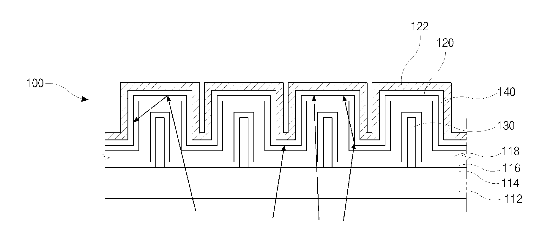
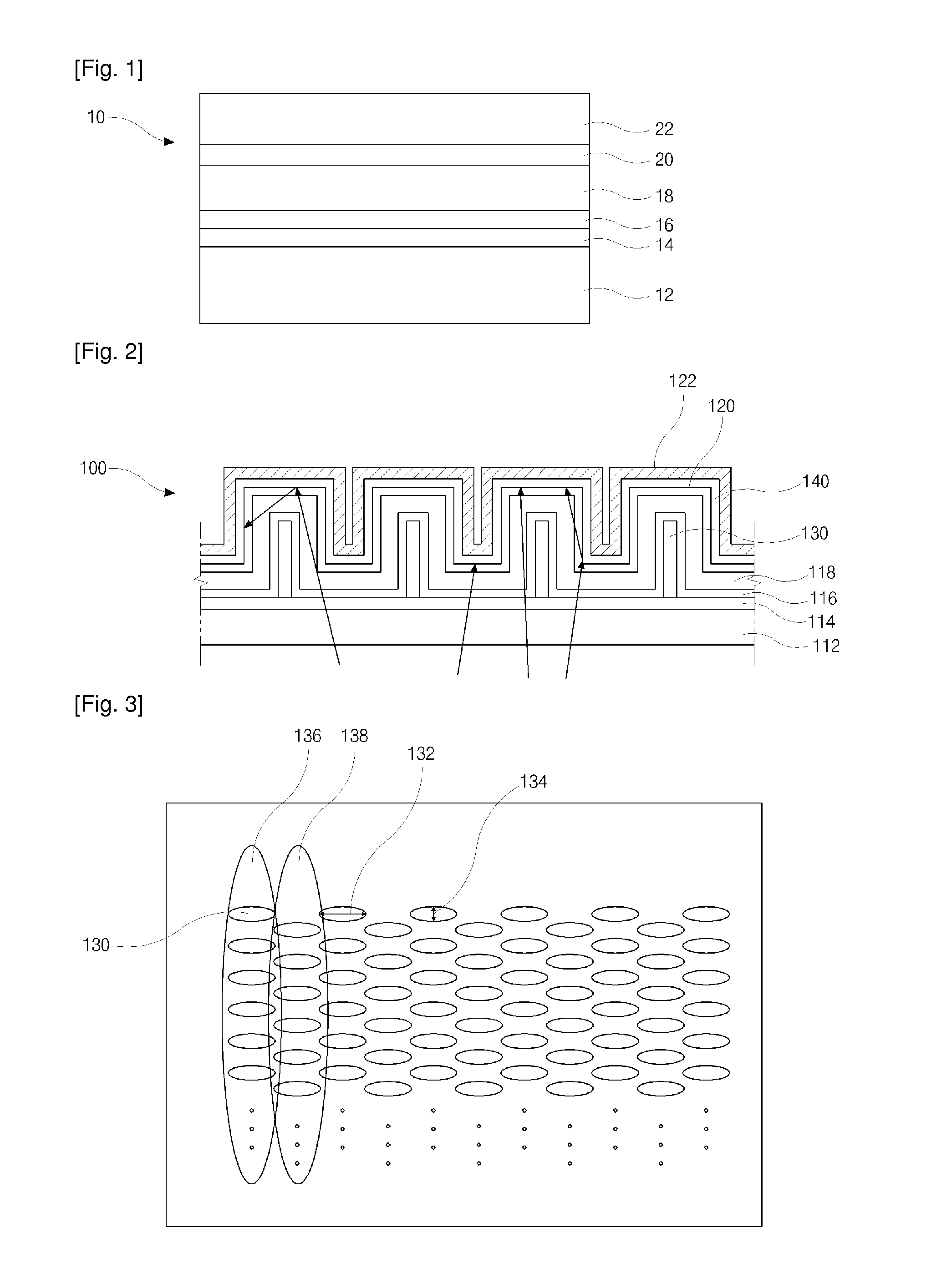
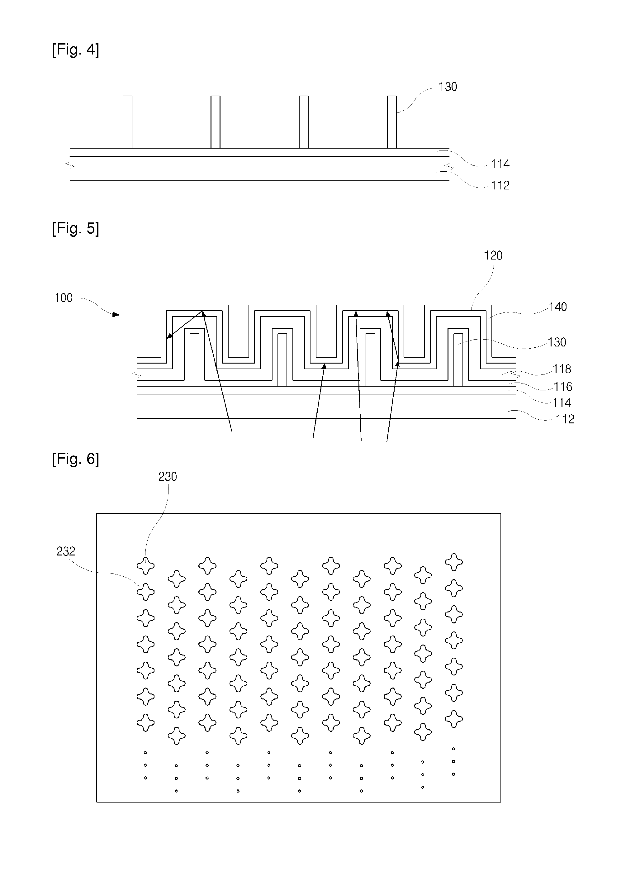
[0030]Referring to FIG. 3, the plurality of pillars 130 having a cylinder shape are disposed on the first electrode 114 (of FIG. 2) of a transparent conductive oxide material. A distance between two adjacent pillars 130 is determined depending on a respective thickness of various layers stacked over the pillars 130. The pillars 130 is formed to maximize a surface area of the intrinsic semiconductor 118 (of FIG. 2) exposed to light. Each of the pillars 130 may have different cross-sectional shape and different arrangement than that of FIG. 2. For example, referring to FIG. 6 showing a plan view of a solar cell according to the present invention, the pillars 230 may have a cross shape in plan. In the cross shape pillar 230, a connecting line between one end of one axis and ends of the other axis has a curved shape 232. Referring back to FIG. 3, the pillars 130 have an oval shape of a major axis 132 and a minor axis 134. The pillars 130 are arranged to be spaced apart from each other b...

first embodiment

[0031]A method of fabricating a solar cell according to the present invention is explained with reference to FIGS. 4 and 5. Referring to FIG. 4, a first electrode 114 is formed on a substrate 112 by depositing a transparent conductive material. For example, the transparent conductive material is deposited by a chemical vapor deposition (CVD) method using tin oxide (SnO2) or zinc oxide (ZnO). Next, a silicon oxide (SiO2) layer (not shown) having a transparent property is deposited on the first electrode 114. Then, the silicon oxide layer (not shown) is patterned by a photolithography to form a plurality of pillars 130. The pillars 130 may be formed of silicon nitride (SiNx) or photoresist. Both silicon nitride (SiNx) and photoresist have a transparent property. To maximize a surface area exposed to light of the intrinsic semiconductor layer (not shown), the pillars 130 is formed of a transparent material having a high optical transmittance. Moreover, the pillars 130 are arranged to h...


PUM


Abstract

A solar cell includes a first electrode on a substrate; a plurality of pillars on the first electrode; a semiconductor layer on the first electrode, wherein a surface area of the semiconductor layer is greater than a surface area of the first electrode; and a second electrode over the semiconductor layer.

Description

TECHNICAL FIELD[0001]The present invention relates to a solar cell, and more particularly, to a solar cell having an improved light absorbing efficiency and a method of fabricating the solar cell.BACKGROUND ART[0002]For response to exhaustion of fossil fuel and preventing environmental pollution, a clean energy source, e.g., solar energy, has been come into the spotlight. Particularly, the solar cell for converting solar energy into electric energy has been developed rapidly. The solar cell may be divided into a solar thermal cell and a photovoltaic solar cell. The solar thermal cell generates steam for rotating a turbine using solar thermal energy, while the photovoltaic solar cell converts solar photons into electric energy using semiconductors.[0003]Among these solar cells, the photovoltaic solar cell, which absorbs light and converts the light into electric energy using an electron of a positive (P) type semiconductor and a hole of a negative (N) type semiconductor, is developed...

Claims


Application Information

Patent Timeline
Patent Type & Authority Applications(United States)
IPC IPC(8): H01L31/0352H01L31/0232H01L31/18
CPCH01L31/035281H01L31/03529H01L31/0392H01L31/056Y02E10/52Y02E10/548H01L31/075H01L31/04H01L31/06H01L31/18
Inventor HONG, JINKIM, JAE-HOSHIN, YONG-WOO
Owner JUSUNG ENG
Why Eureka
Try Eureka