Method and apparatus for manufacturing epitaxial silicon wafer

a manufacturing apparatus and epitaxial silicon technology, applied in the direction of crystal growth process, polycrystalline material growth, chemically reactive gas, etc., can solve the problems of difficult to monitor the temperature of the outer circumferential portion and a nearby vicinity in consideration of the structure of the manufacturing apparatus, and not necessarily effective, so as to achieve satisfactory epitaxial wafer, reduce the effect of dislocation and less defects

Active Publication Date: 2010-06-10
SUMCO TECHXIV
View PDF16 Cites 22 Cited by
  • Summary
  • Abstract
  • Description
  • Claims
  • Application Information

AI Technical Summary

Benefits of technology

[0029]According to the present invention, it is possible to effectively prevent dislocation that occurs...

Problems solved by technology

However, while the temperature control, which is effective if the flow rate of a carrier gas and/or a raw material gas and the output of high-frequency inductive heater or the like are controlled at the same time, may not apply in the same way in the case where the flow rate remains constant or heat is provided by another kind of heater (for example, a halogen lamp), and moreover, it is not easy to control the temperature adjustment since the semiconductor wafer is heated by the heat from the susceptor.
On the other hand, prevention of the slip dislocation by conducting a heat treatment in a state that a temperature of at least a contact portion of the semicon...

Method used


Image

  • Method and apparatus for manufacturing epitaxial silicon wafer
  • Method and apparatus for manufacturing epitaxial silicon wafer
  • Method and apparatus for manufacturing epitaxial silicon wafer

Examples


Embodiment Construction

[0042]Next, an embodiment of the present invention is now described with reference to the accompanying drawings. Components of like configuration or like function and corresponding portions thereof are referred to by common symbols throughout the drawings and their description may be omitted. And the following description also shows merely examples of embodiments according to the present invention such that modifications can be made appropriately based on the common general technical knowledge of the one skilled in the art without departing from the scope of the present invention. Therefore, the scope of the present invention is not limited to these specific examples. Further, the drawings are presented in an exaggerated way for the explanation such that components are not necessarily drawn true to the scale of the real one.

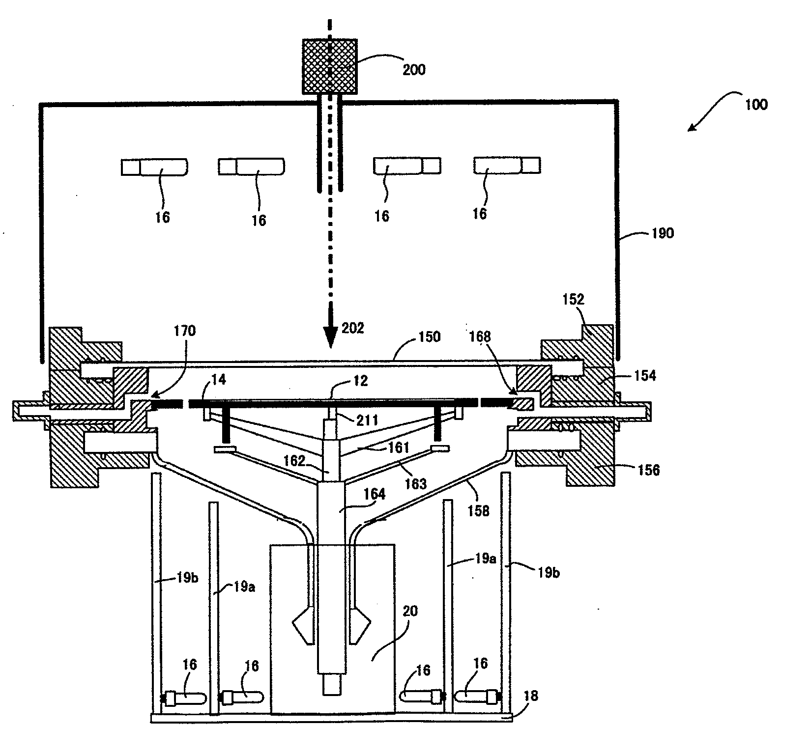
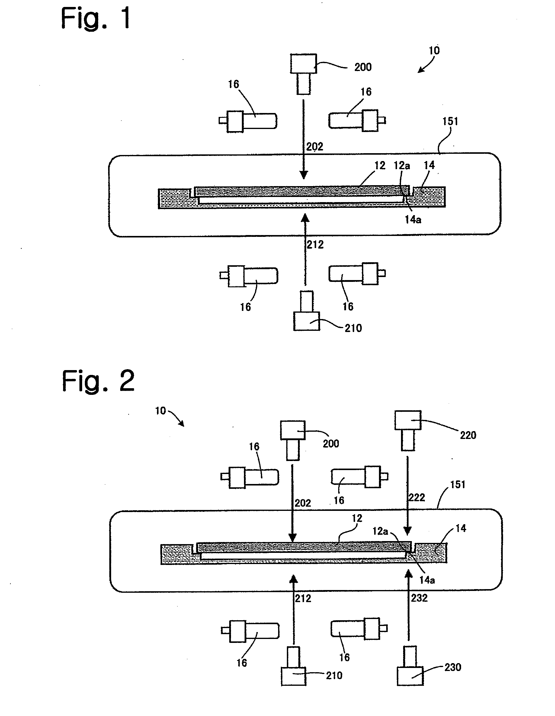
[0043]FIG. 1 is a schematic diagram of an epitaxial wafer manufacturing apparatus 10, which relates to an embodiment of the present invention. A silicon wafer se...


PUM

PropertyMeasurementUnit
Temperatureaaaaaaaaaa

Abstract

A method of manufacturing an epitaxial wafer in which an epitaxial layer is grown over a main surface of a silicon wafer placed substantially horizontally on a susceptor is provided. The method comprises: a growing step of the epitaxial layer; and a cooling step of cooling the epitaxial wafer having the epitaxial layer. The cooling step comprises: a wafer measurement step of measuring a temperature of the epitaxial wafer; a susceptor measurement step of measuring a temperature of the susceptor; and a control step of controlling a heater capable of heating at least the susceptor or the epitaxial wafer such that difference between a temperature of the epitaxial wafer and a temperature of the susceptor is within a predetermined range.

Description

CROSS REFERENCE TO RELATED APPLICATIONS[0001]This application is based upon and claims the benefits of priorities from Japanese Patent Applications No. 2008-315108 and 2008-315109 both filed on Dec. 10, 2008, the entire contents of which are incorporated herein by reference.FIELD OF THE INVENTION[0002]The present invention relates to a method and an apparatus for manufacturing an epitaxial silicon wafer, which may be utilized in devices or the like of semiconductor integrated circuits. In particular, it relates to the method and the apparatus for manufacturing the epitaxial silicon wafer while a temperature of the wafer is controlled on an occasion of epitaxial growth.BACKGROUND ART[0003]As high-density packaging of integrated circuit devices of silicon semiconductors continues to make rapid advancements, higher quality of silicon wafers for the devices is increasingly in demand. That is, crystal defects such as dislocation causing an increase of leak current and a reduction of carr...

Claims


Application Information

Patent Timeline
IPC IPC(8): C23C16/52C23C16/00
CPCC23C16/4583C23C16/481C30B29/06C30B25/16C30B25/10C23C16/52H01L21/67248
Inventor NARAHARA, KAZUHIRO
Owner SUMCO TECHXIV
Why Eureka
Try Eureka