
Method for manufacturing nitride semiconductor device

Active Publication Date: 2010-06-17
MITSUBISHI ELECTRIC CORP
View PDF2 Cites 2 Cited by
  • Summary
  • Abstract
  • Description
  • Claims
  • Application Information

AI Technical Summary

Benefits of technology

[0007]To solve such problems, it is an object of the present invention to provide a method for manufacturing a nitride semiconductor device that can prevent the cracking of the GaN substrate during the vacuum suction.
[0009]According to the present invention, the cracking of the GaN substrate during the vacuum suction can be prevented.

Problems solved by technology

The epitaxial deposit caused a problem of the cracking of the GaN substrate when the N surface of the GaN substrate is subjected to vacuum suction with the vacuum suction apparatus.
Therefore, if an epitaxial deposit is present on the N surface of a GaN substrate, a problem, wherein diffused reflection was generated and the transcription process became unstable, was caused.

Method used


Image

  • Method for manufacturing nitride semiconductor device
  • Method for manufacturing nitride semiconductor device
  • Method for manufacturing nitride semiconductor device

Examples


first embodiment

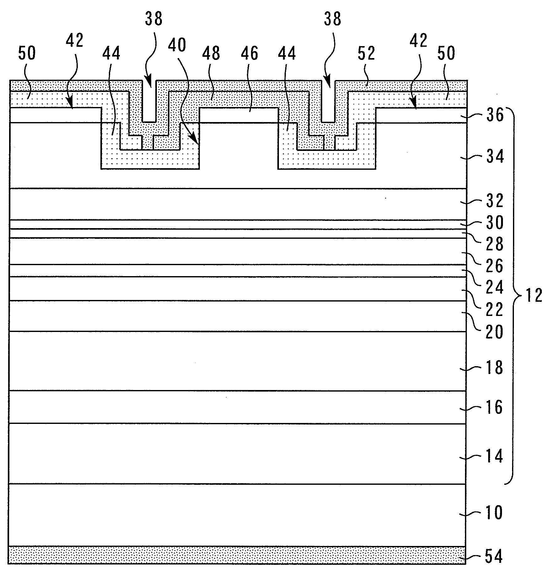
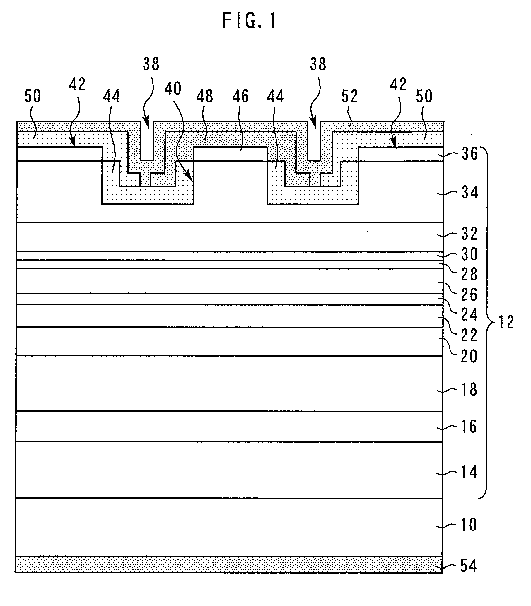
[0016]FIG. 1 is a sectional view showing a nitride semiconductor device according to the first embodiment of the present invention. The nitride semiconductor device is a blue-violet laser diode of a waveguide ridge type.

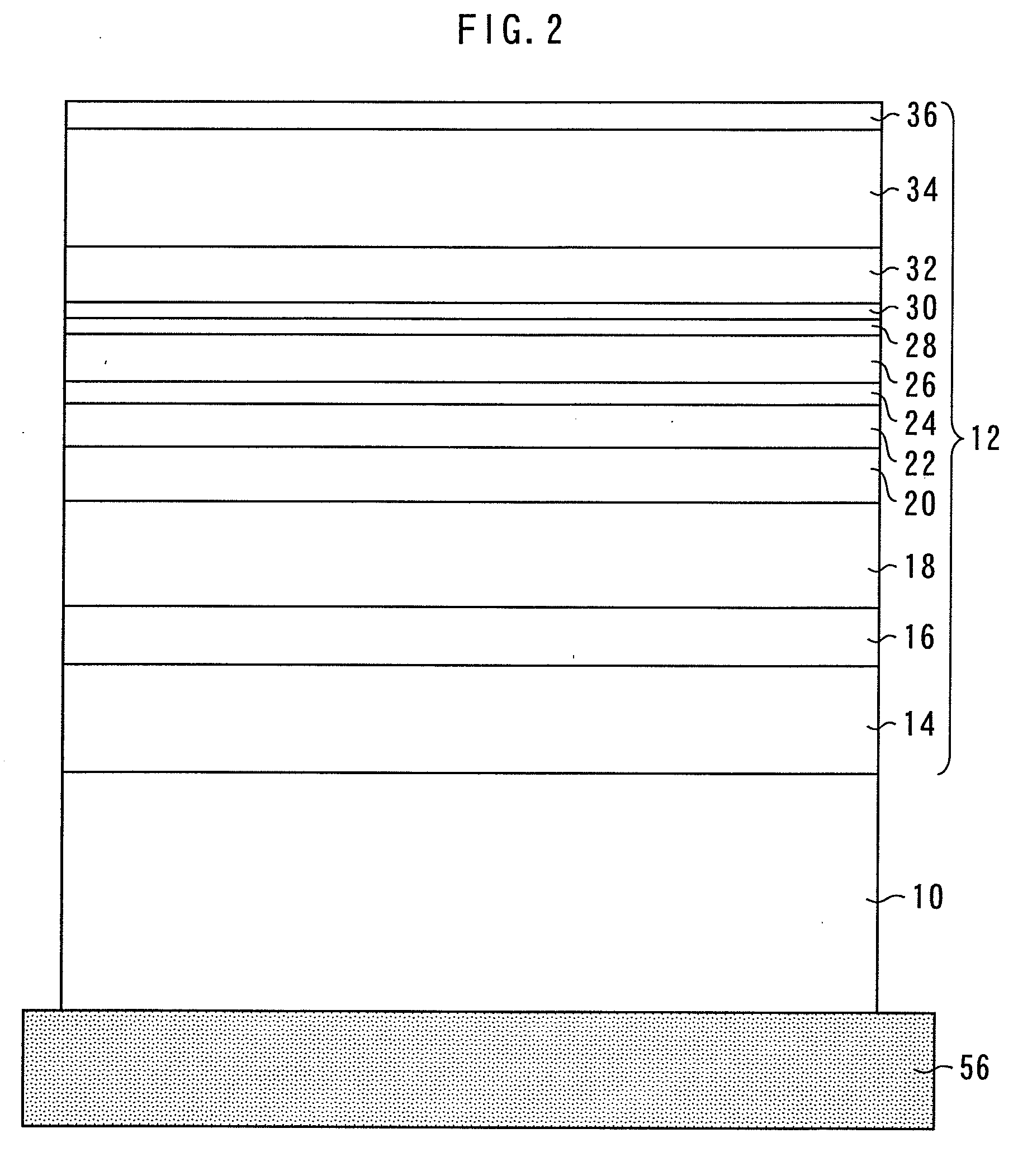
[0017]On the Ga surface of an n-type GaN substrate 10, as a semiconductor layer 12 formed of GaN-based materials, an n-type GaN buffer layer 14 having a thickness of 1 μm, an n-type Al0.07Ga0.93N clad layer 16 having a thickness of 400 nm, an n-type Al0.045Ga0.955N clad layer 18 having a thickness of 1000 nm, an n-type Al0.015Ga0.985N clad layer 20 having a thickness of 300 nm, an n-type GaN light guiding layer 22 having a thickness of 80 nm, an n-side SCH (Separate Confinement Hetero structure) layer 24 formed of In0.02Ga0.98N having a thickness of 30 nm, an active layer 26, a p-side SCH layer 28 formed of In0.02Ga0.98N having a thickness of 30 nm, a p-type Al0.2Ga0.8N electron barrier layer 30 having a thickness of 20 nm, a p-type GaN light guiding layer 32 having ...

second embodiment

[0046]In the second embodiment, as shown in FIG. 18, the epitaxial deposit 58 is removed by the dry etching of the N surface of the n-type GaN substrate 10 using an etching gas such as SiCl4, C12, and Ar. Otherwise, the second embodiment is identical to the first embodiment. Although the epitaxial deposit 58 formed of a GaN-based material is difficult to be removed by wet etching, it can be removed by dry etching. Therefore, an equivalent effect as in the first embodiment can be obtained.

third embodiment

[0047]In the third embodiment, as shown in FIG. 19, the epitaxial deposit 58 is removed by selectively etching the N surface relative to the Ga surface of the n-type GaN substrate 10 using KOH. However, a material that is not dissolved in KOH, such as an insulating film and a metal film, is used as the protective film 60. Otherwise, the second embodiment is identical to the first embodiment.

[0048]KOH does not corrode the Ga surfaces of the n-type GaN substrate 10 and the semiconductor layer 12, and selectively etches the N surface of the n-type GaN substrate 10. Thereby, the epitaxial deposit 58 can be peeled in a liftoff manner. Therefore, an equivalent effect as in the first embodiment can be obtained.


PUM


Abstract

A method for manufacturing a nitride semiconductor device, comprises epitaxially growing a semiconductor layer of a GaN-based material on the Ga surface of a GaN substrate while the GaN substrate is mounted on a substrate holder the substrate warping during the epitaxial growth so that a epitaxial deposit is deposited on the N surface of the substrate; and subjecting the N surface of the GaN substrate to vacuum suction after the epitaxial growth of the semiconductor layer; removing the epitaxial deposit from the N side of the GaN substrate after the semiconductor layer has been epitaxially grown, and before the N surface of the n-type GaN substrate is subjected to vacuum suction.

Description

BACKGROUND OF THE INVENTION[0001]1. Field of the Invention[0002]The present invention relates to a method for manufacturing a nitride semiconductor device manufactured by the epitaxial growth of a semiconductor layer formed of a GaN-based material on the Ga surface of a GaN substrate in a state wherein the GaN substrate is mounted on a substrate holder, and the vacuum suction of the N surface of the GaN substrate with a vacuum suction apparatus. More specifically, the present invention relates to a method for manufacturing a nitride semiconductor device that can prevent the cracking of the GaN substrate during the vacuum suction.[0003]2. Background Art[0004]GaN-based materials have been attracting attention as the materials for a blue light-emitting element (for example, refer to Japanese Patent Laid-Open No. 2008-251683). A semiconductor layer formed of a GaN-based material is epitaxially grown on the Ga surface of a GaN substrate in a state wherein the GaN substrate is mounted on ...

Claims


Application Information

Patent Timeline
IPC IPC(8): H01L21/20
CPCB82Y20/00H01S5/0425H01S5/2009H01S5/34333H01S5/2214H01S5/3211H01S5/22H01S2301/176H01S5/04252H01S5/04254Y10S117/915
Inventor ABE, SHINJIKAWASAKI, KAZUSHIGE
Owner MITSUBISHI ELECTRIC CORP
Learn More