Circuit and method for correcting skew in a plurality of communication channels for communicating with a memory device, memory controller, system and method using the same, and memory test system and method using the same

a plurality of communication channels and circuits, applied in the field of memory circuits and systems, memory controller circuits and systems, memory testing circuits and systems, etc., can solve the problems of difficult or impossible testing of ddr3 memory circuits, and achieve the effect of reducing or eliminating skew among channels

Active Publication Date: 2010-06-17
MGP MFG +1
View PDF5 Cites 33 Cited by
  • Summary
  • Abstract
  • Description
  • Claims
  • Application Information

AI Technical Summary

Benefits of technology

[0009]The present inventive concept obviates one or more limitations of the prior art by reducing or eliminating skew among channels used to communicate with a high-speed memory circuit, for example, a DDR3 DRAM memo

Problems solved by technology

This “skew” in the propagation times can introduce errors in the process of testing the DUT.
In fact, at such high-speed operation, because of the channel skew, the control and data signals tr

Method used


Image

  • Circuit and method for correcting skew in a plurality of communication channels for communicating with a memory device, memory controller, system and method using the same, and memory test system and method using the same
  • Circuit and method for correcting skew in a plurality of communication channels for communicating with a memory device, memory controller, system and method using the same, and memory test system and method using the same
  • Circuit and method for correcting skew in a plurality of communication channels for communicating with a memory device, memory controller, system and method using the same, and memory test system and method using the same

Examples


Embodiment Construction

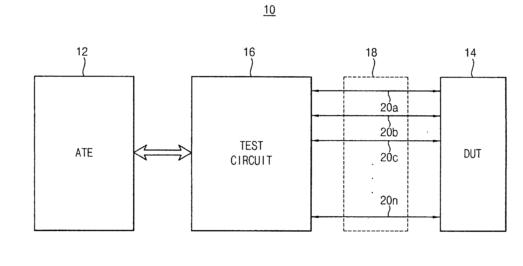
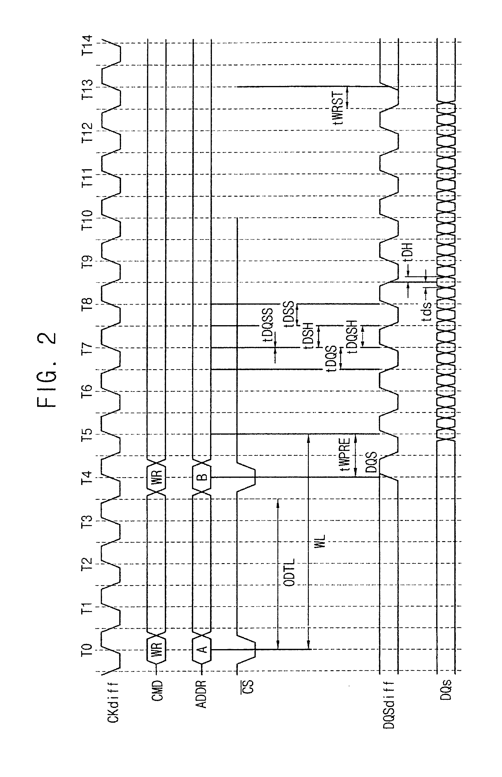
[0109]FIG. 2 is a timing diagram illustrating timing during a write operation in a test system for testing a DDR3 DRAM memory circuit. The timing diagram illustrates the clock signal CKdiff, the CMD and ADDR signals, a / CS signal, the data signals DQs and the data strobe signal DQSdiff. These are the standard signals used in DDR3 DRAM memory and are based on the standard DDR3 requirements. In the test system, as illustrated in FIG. 1, these signals are transferred along the channels 20a-20n of the interface 18 to simulate communication with the DDR3 memory circuit 14. As illustrated in the timing diagram of FIG. 2, when skew is present between channels in the test environment, for example, over 200 ps skew among the channels, then the test system testing the DDR3 DRAM will not meet the timing requirements of DDR3, and the testing will not function properly. Similarly, during a read operation, because of the skew among the channels, it is difficult to sense the DDR3 output with accur...


PUM


Abstract

In a circuit and method for correcting skew among a plurality of communication channels used in communicating with a memory circuit, and in a memory controller and memory controlling method, and in a memory system and method, the circuit for correcting skew includes a transmitting circuit for transmitting a reference signal to input ends of the plurality of channels and through the plurality of channels, and a plurality of receiving circuits for receiving at the input ends of the plurality of channels a respective plurality of reflected signals, the reflected signals being reflected from respective output ends of the plurality of channels. A detection circuit receives the reflected signals and detects relative signal propagation time differences between the plurality of channels. A delay circuit coupled to at least one of the channels sets a signal propagation delay in the at least one of the channels based on the detected relative signal propagation time differences.

Description

RELATED APPLICATION[0001]This application relies for priority under 35 U.S.C. 119(a) on Korean Patent Application number 10-2008-0127103, filed in the Korean Intellectual Property Office on Dec. 15, 2008, the entire contents of which are incorporated herein by reference.BACKGROUND[0002]1. Field of the Invention[0003]This application relates to memory circuits and systems, memory controller circuits and systems and memory testing circuits and systems, and, more particularly, to memory circuits and systems, memory controller circuits and systems and memory testing circuits and systems in which skew among multiple communication channels is substantially reduced or eliminated.[0004]2. Description of the Related Art[0005]In the fabrication of memory circuits and devices, it is necessary to test the memory circuit or device. This is typically accomplished using automatic test equipment (ATE) coupled to the memory circuit or device, i.e., the device under test (DUT). The ATE generates and ...

Claims


Application Information

Patent Timeline
IPC IPC(8): G11B20/20G06F11/00
CPCG11C29/02G11C29/028G11C29/023G11C29/022H04L7/02H04B1/10H04L12/28
Inventor JANG, YOUNG-CHAN
Owner MGP MFG
Why Eureka
Try Eureka