Fine wiring package and method of manufacturing the same

a technology of fine wiring and manufacturing methods, applied in the field of fine wiring packages, can solve the problems of difficult to form conducting holes and inability to form wiring having a high reliability, and achieve the effect of convenient operation

Active Publication Date: 2010-06-24
SHINKO ELECTRIC IND CO LTD
View PDF13 Cites 25 Cited by
  • Summary
  • Abstract
  • Description
  • Claims
  • Application Information

AI Technical Summary

Benefits of technology

[0024]Exemplary embodiments of the present invention provide a manufacturing method capable of obtaining a suitable package for a fine wiring in which a terminal surface of an electronic component constituting the package is set to have a uniform height to easily carry out an electrical connection of a terminal and a wiring through a conducting hole connected to each terminal, and the package is formed in a supporting state on a support to prevent a position of each portion from being shifted till a final stage of a package manufacturing process, and a fine wiring package thus manufactured.

Problems solved by technology

Since the support is peeled from the package, a warpage occurs over the package so that the terminal surface is not flattened.
Consequently, it is hard to form the conducting hole.
To the contrary, if the temporary bond of the support and the element is set slightly strongly, there is a problem in that the adhesive itself sticks to the terminal, concavo-convex portions are generated on the sealing resin surface due to the curing and shrinkage of the sealing resin and the terminal surface is not flattened, and a warpage occurs and the terminal surface is not flattened because the support is peeled.
When the insulating layer is to be formed on the sealing resin, moreover, there is a problem in that concavo-convex portions are generated on the insulating resin corresponding to a height of the terminal of the electronic component exposed from the sealing resin, a defect is caused in a subsequent formation of a wiring and a wiring having a high reliability cannot be formed.

Method used


Image

  • Fine wiring package and method of manufacturing the same
  • Fine wiring package and method of manufacturing the same
  • Fine wiring package and method of manufacturing the same

Examples


Embodiment Construction

[0056]Exemplary embodiments according to the invention will be described below in detail with reference to the accompanying drawings.

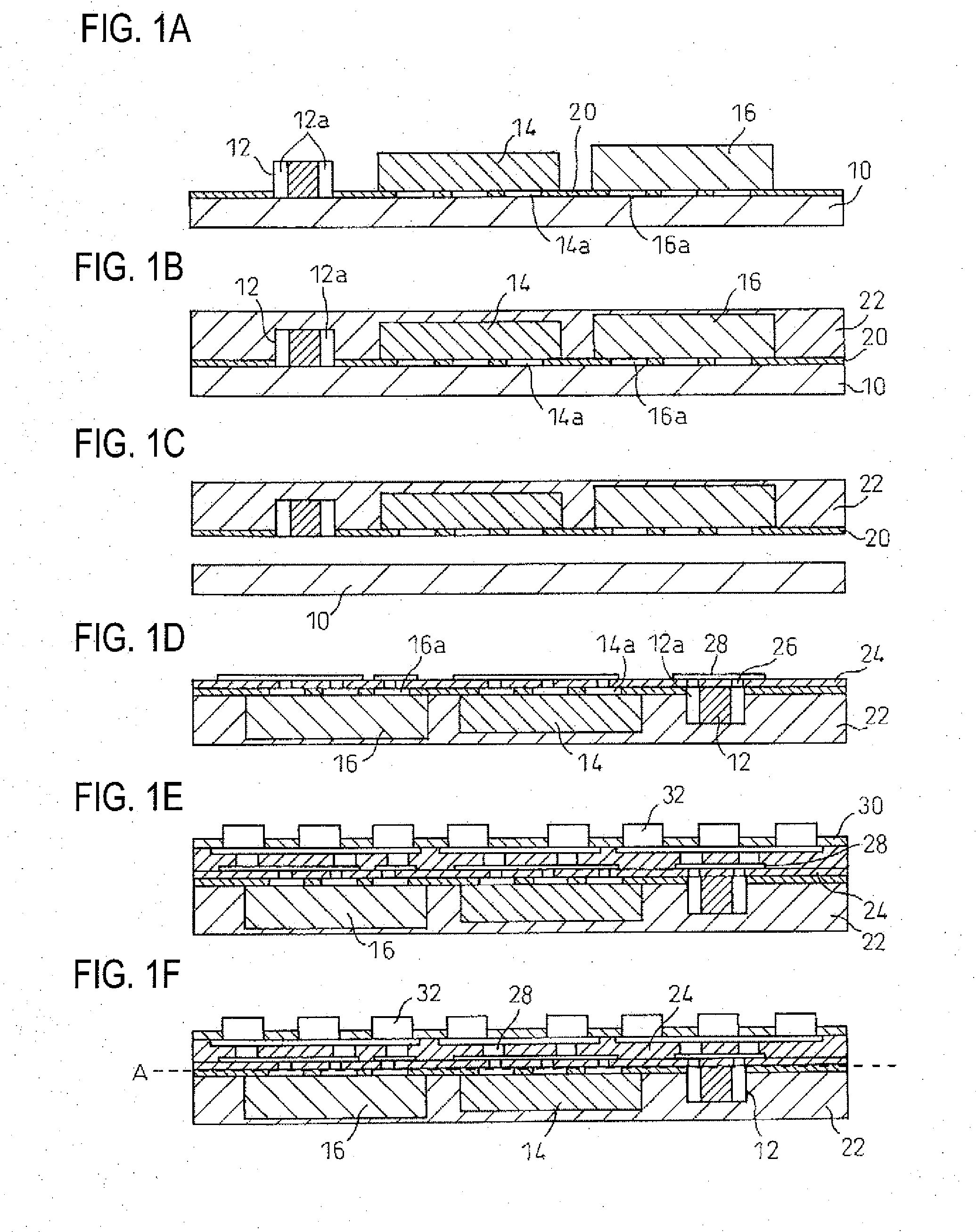
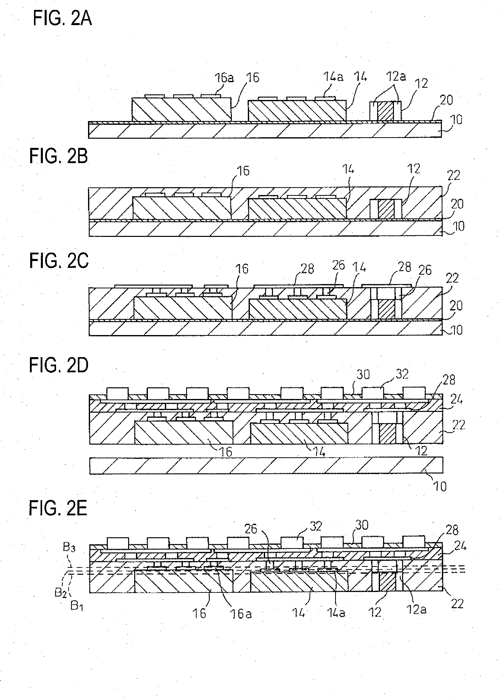
[0057]FIGS. 3A to 3D, FIGS. 4A to 4E and FIGS. 5A and 5B show an embodiment of a method of manufacturing a fine wiring package according to the invention.

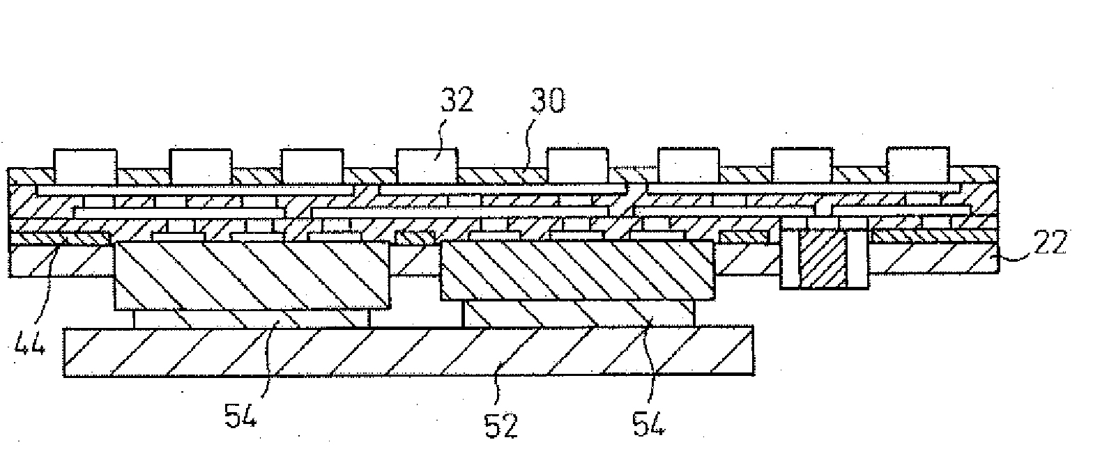
[0058]Each of electronic components such as a passive element 12 and active elements 14 and 16 has one surface which is flat (a first surface), and the other surface (a second surface) to be a back face which is also formed as a flat surface which is parallel with the first surface. The electronic components have a plurality of electrode terminals 12a, 14a and 16a on the first surfaces respectively. Surfaces of the electrode terminals 12a, 14a and 16a of the respective electronic components are also formed to be positioned on a constant plane for each component.

[0059]In FIG. 3A, the passive element 12 and the active elements 14 and 16 are provided on a first support 10 through an adhesive layer 20. Th...


PUM

PropertyMeasurementUnit
bonding forceaaaaaaaaaa
conductiveaaaaaaaaaa
insulatingaaaaaaaaaa

Abstract

At least one electronic component having a plurality of terminals on one of surfaces is temporarily fixed to a surface of a first support with a first adhesive layer in such a manner that the terminal side of the electronic component faces the first support. A second support having a second adhesive layer is fixed to the electronic component in order to interpose the electronic component between the first support and the second support. The first support and the first adhesive layer are peeled. The electronic component on the second support is sealed with a sealing resin in such a manner that at least a part of the terminals of the electronic component is exposed. An insulating resin layer and a wiring layer to be electrically connected to the terminal of the electronic component are stacked on the electronic component and the sealing resin.

Description

[0001]This application claims priority to Japanese Patent Application No. 2008-328488, filed Dec. 24, 2008, in the Japanese Patent Office. The Japanese Patent Application No. 2008-328488 is incorporated by reference in its entirety.TECHNICAL FIELD[0002]The present disclosure relates to a semiconductor package and more particularly to a fine wiring package which can be used as a general package of a semiconductor integrated circuit and a method of manufacturing the fine wiring package.RELATED ART[0003]Usually, at least one active element or passive element is fixed onto a fine wiring package through a sealing resin. A wiring layer and an insulating resin layer are stacked on the individual active element or passive element.[0004]In a method of manufacturing the fine wiring package which includes at least one active element or passive element, a support is used and each element is provided on the support through an adhesive layer and is sealed with a resin, a wiring layer and an insul...

Claims


Application Information

Patent Timeline
Patent Type & Authority Applications(United States)
IPC IPC(8): H05K1/16H05K3/30
CPCH01L2924/01006H01L2924/14H01L24/96H05K3/4602H01L21/568H05K2203/1469H01L2924/19105H01L2221/68359H01L2221/68345H01L2924/01033H01L24/82H01L2224/24137H01L21/6835H01L24/18H05K3/4644H05K1/185H01L2224/32245H01L23/3121H01L2224/18H05K2203/0152H01L2224/73267Y10T29/49162H01L2924/15153H05K2203/1476H01L2224/24195H01L2924/01005Y10T29/4913H01L24/19H01L2224/12105H01L2924/18162H01L2924/00014H01L2924/3511H01L2224/04105H01L2224/9222H01L2224/92244H01L2224/05599H01L2924/00H01L2224/0555H01L2224/0556H01L2224/05573H01L2224/05568H01L2224/0554
Inventor KUNIMOTO, YUJITATEIWA, AKIHIKO
Owner SHINKO ELECTRIC IND CO LTD
Why Eureka
Try Eureka