Semiconductor device having saddle fin-shaped channel and method for manufacturing the same

a technology of semiconductor devices and fins, which is applied in the direction of semiconductor devices, semiconductor/solid-state device details, electrical apparatus, etc., can solve the problems of enlargement of the recess pattern defined in the isolation layer, difficult to achieve the desired target threshold voltage, and the design rule of semiconductor devices is reduced

Inactive Publication Date: 2010-07-01
SK HYNIX INC
View PDF14 Cites 27 Cited by
  • Summary
  • Abstract
  • Description
  • Claims
  • Application Information

AI Technical Summary

Benefits of technology

[0009]Embodiments of the present invention include a semiconductor device which can prevent a bridge from occurring between a gate pattern and an LPC plug during the formation of a saddle fin-shaped channel, and a method for manufacturing the same.
[0010]Also, embodiments of the present invention include a semiconductor device in which the manufacturing yield is improved by preventing a bridge from occurring between a gate pattern and an LPC plug, and a method for manufacturing the same.
[0018]In another aspect of the present invention, a method for manufacturing a semiconductor device includes the steps of forming active regions and an isolation layer on a semiconductor substrate such that the isolation layer delimits the active regions; etching the active regions and the isolation layer to a first depth; defining recess patterns for gates by additionally etching portions of the isolation layer which are etched to the first depth, to a second depth; enlarging a width of upper parts of the recess patterns for gates, which are defined in the isolation layer; forming gate patterns in and over the recess patterns for gates; and forming a gate spacer to cover the gate patterns. The gate patterns are formed to have a width less than that of the enlarged upper parts of the recess patterns for gates, which are defined in the isolation layer. The gate spacer fills the gaps that are created between the gate patterns and the enlarged upper parts of the recess patterns for gates, which are defined in the isolation layer.

Problems solved by technology

Trends in the semiconductor industry have lead to a decrease in the design rule of a semiconductor device.
This decrease has made it difficult to achieve the desired target threshold voltage when using a conventional planar channel structure.
In this regard, enlargement of the recess pattern defined in the isolation layer is likely due to etch loss caused during the pre-cleaning process.
Due to this fact, a self-align contact (SAC) fail, such as bridging between a gate pattern and an LPC plug, can occur, thereby leading to a decrease in manufacturing yield.

Method used


Image

  • Semiconductor device having saddle fin-shaped channel and method for manufacturing the same
  • Semiconductor device having saddle fin-shaped channel and method for manufacturing the same
  • Semiconductor device having saddle fin-shaped channel and method for manufacturing the same

Examples


Embodiment Construction

[0060]Hereafter, specific embodiments of the present invention will be described in detail with reference to the accompanying drawings.

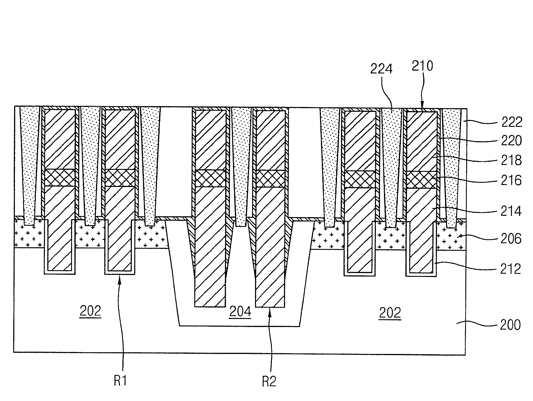
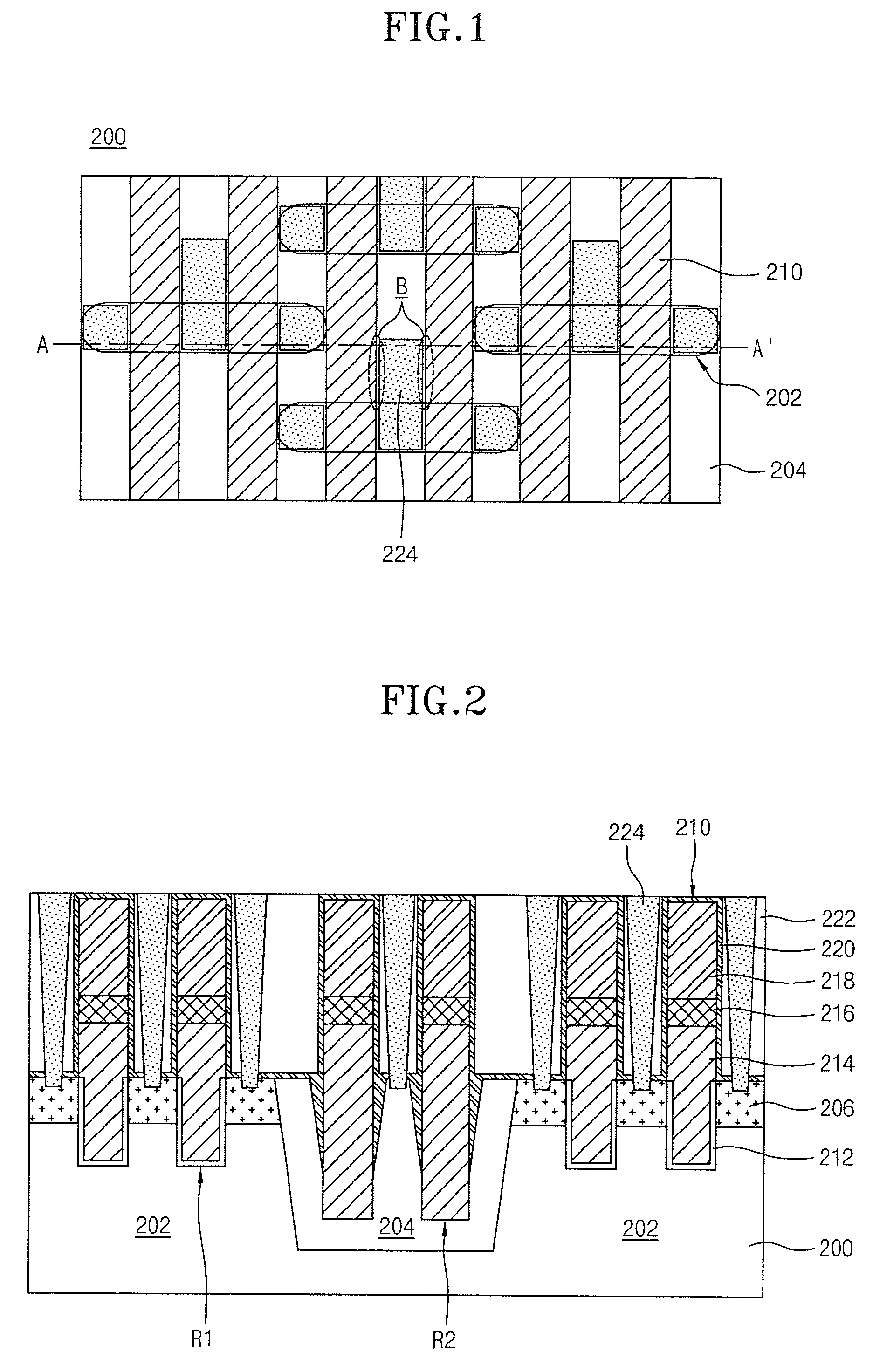
[0061]FIG. 1 is a plan view showing a semiconductor device in accordance with an embodiment of the present invention, and FIG. 2 is a cross-sectional view taken along the line A-A′ of FIG. 1.

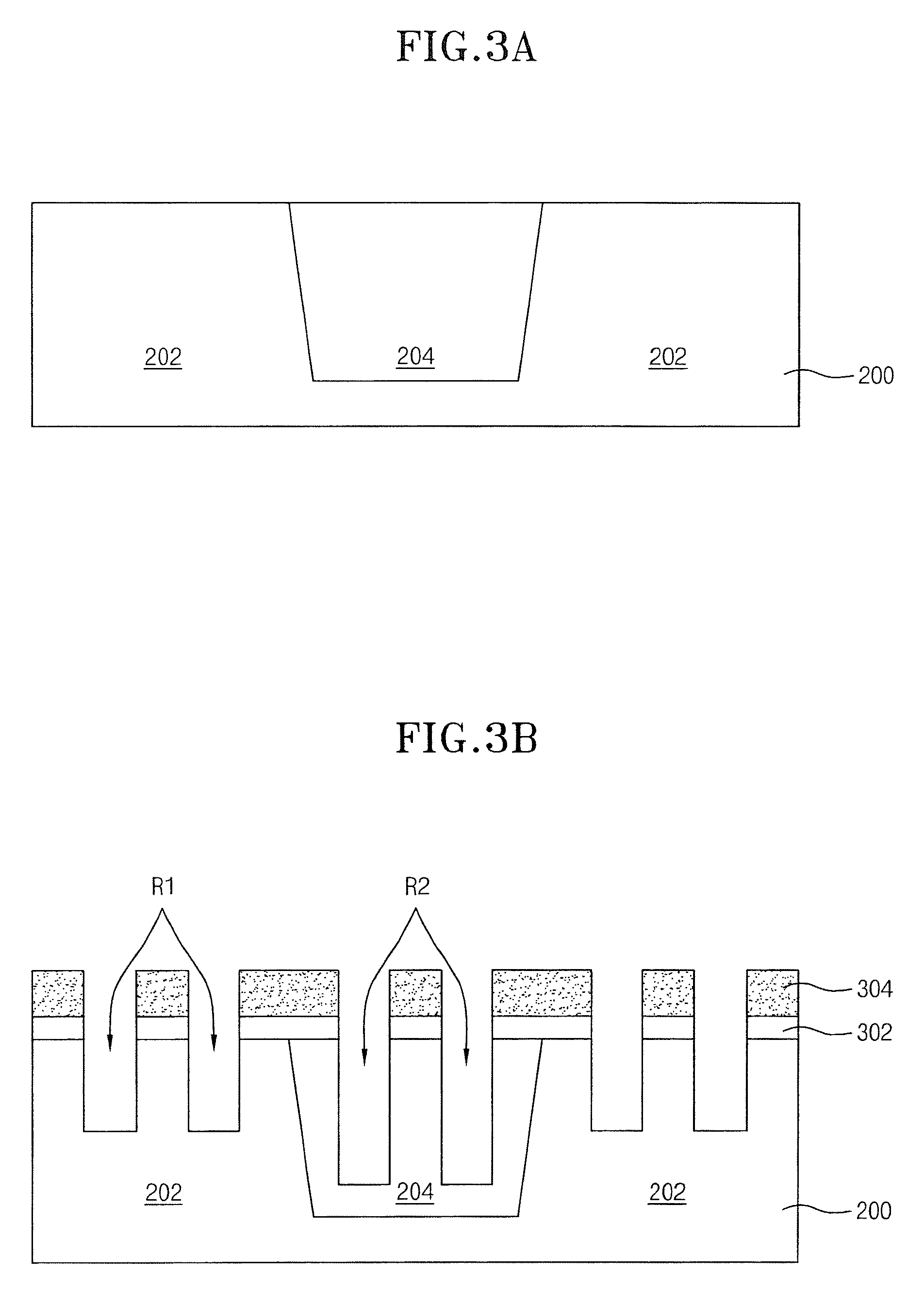
[0062]Referring to FIGS. 1 and 2, an isolation layer 204 is formed in a semiconductor substrate 200 to delimit active regions 202. A plurality of first recess patterns R1 are defined to a first depth in gate forming areas of the active regions 202, and second recess patterns R2 are defined to a depth greater than the first depth in the portions of the isolation layer 204 that extend out from the gate forming areas of the active regions 202 such that the front and rear surfaces of the gate forming areas are exposed (e.g., portions of the active region at the front and rear of the gate forming areas of the active regions 202 are exposed) and saddle fin-shaped chann...


PUM


Abstract

A semiconductor device includes a semiconductor substrate with an isolation layer formed in the semiconductor substrate to delimit active regions. Recess patterns for gates are defined in the active regions and the isolation layer. Gate patterns are formed in and over the recess patterns for gates, and a gate spacer is formed to cover the gate patterns. The recess patterns for gates have a first depth in the active regions and a second depth, which is greater than the first depth, in the isolation layer. Gaps are created between the gate patterns and upper parts of the recess patterns for gates that are defined in the isolation layer. The gate spacer fills the gaps and protects the gate spacer so as to prevent bridging.

Description

CROSS-REFERENCE TO RELATED APPLICATIONS[0001]The present application claims priority to Korean patent application number 10-2008-0137358 filed on Dec. 30, 2008, which is incorporated herein by reference in its entirety.BACKGROUND OF THE INVENTION[0002]The present invention relates to a semiconductor device, and more particularly, to a semiconductor device having a saddle fin-shaped channel and a method for manufacturing the same.[0003]Trends in the semiconductor industry have lead to a decrease in the design rule of a semiconductor device. This decrease has made it difficult to achieve the desired target threshold voltage when using a conventional planar channel structure. A semiconductor device with a three-dimensional channel structure has been suggested as a device with potential for overcoming the problems associated with the convention planar channel structure. Examples of a semiconductor device having a three-dimensional channel structure include semiconductor devices having a...

Claims


Application Information

Patent Timeline
Patent Type & Authority Applications(United States)
IPC IPC(8): H01L23/58H01L21/76
CPCH01L21/823437H01L21/823481H01L21/76224H01L29/4236H01L29/66621
Inventor CHAE, KWANG KEEYU, JAE SEONLEE, JAE KYUN
Owner SK HYNIX INC
Why Eureka
Try Eureka