Output driver for use in semiconductor device

Inactive Publication Date: 2010-07-01
SK HYNIX INC
View PDF6 Cites 26 Cited by
  • Summary
  • Abstract
  • Description
  • Claims
  • Application Information

AI Technical Summary

Benefits of technology

[0019]Embodiments of the present invention are directed to an output driver for use in a semiconductor devi

Problems solved by technology

However, the pull-down NMOS transistor PD_NMOS receiving the pull-down drive control signal PD_DRV_CTRL of the logic low level is turned off and cannot provide the output terminal DQ with the ground voltage VSS.
In other words, if the resistance of the output terminal DQ of the DDR3 SDRAM is out of the range of “34Ω±10%”, the reliable data transmission cannot be en

Method used


Image

  • Output driver for use in semiconductor device
  • Output driver for use in semiconductor device
  • Output driver for use in semiconductor device

Examples


Example

[0029]Other objects and advantages of the present invention can be understood by the following description, and become apparent with reference to the embodiments of the present invention.

[0030]Hereinafter, an output driver for use in a semiconductor device in accordance with an embodiment of the present invention will be described in detail.

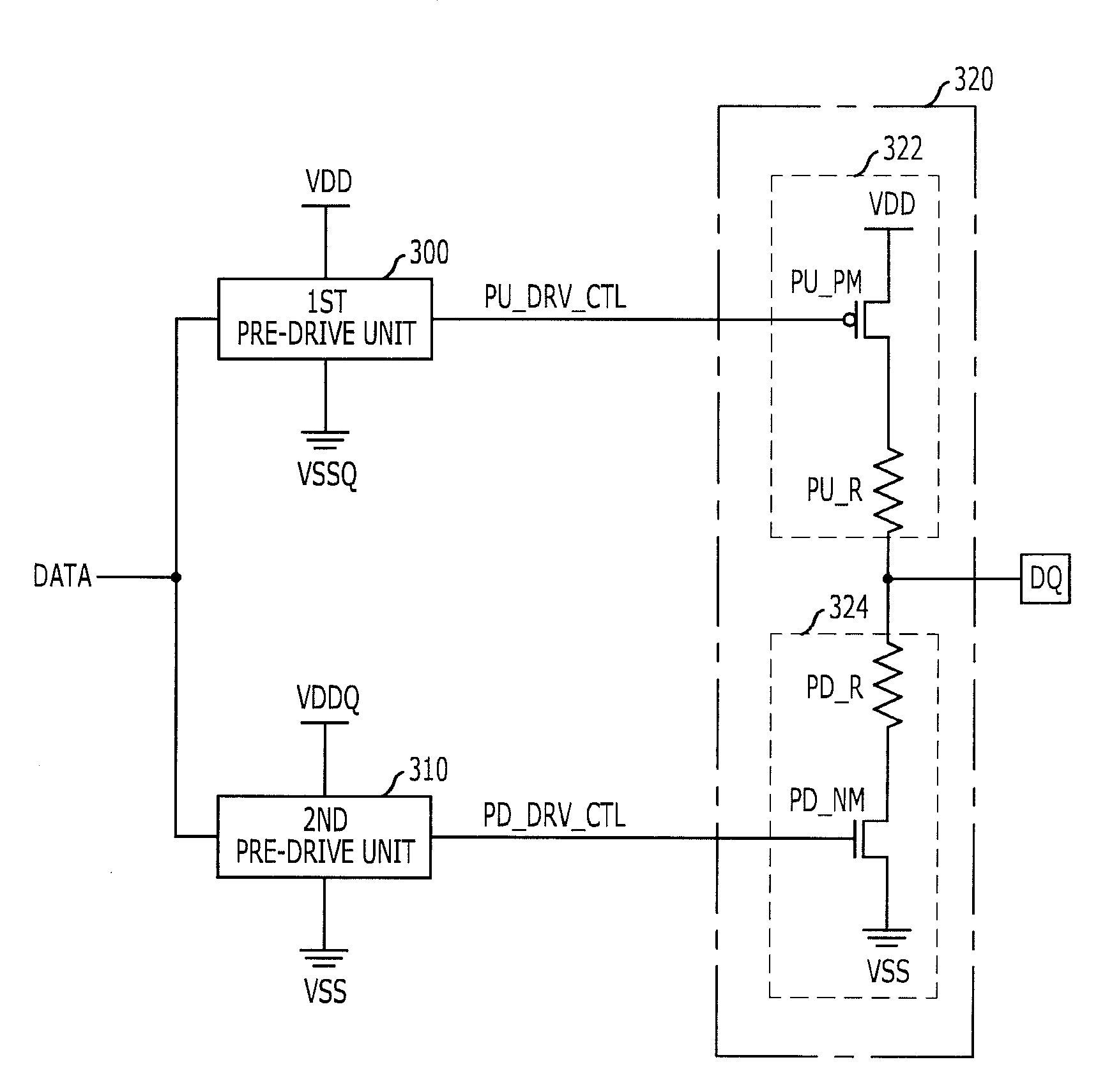
[0031]FIG. 3 is a block diagram illustrating an output driver for use in a semiconductor device in accordance with an embodiment of the present invention.

[0032]Referring to FIG. 3, the output driver includes a first pre-drive unit 300, a second pre-drive unit 310, and a main drive unit 320.

[0033]The first pre-drive unit 300 receives a data signal DATA swinging between a power supply voltage VDD level and a ground voltage VSS level. Then, the first pre-drive unit 300 generates a pull-up drive control signal PU_DRV_CTL, swinging between the power supply VDD voltage level and a low voltage VBBQ level based on the data signal DATA. Herein, the low vo...


PUM


Abstract

An output driver for use in a semiconductor device includes a first pre-drive unit, a second pre-drive unit, and a main drive unit. The first pre-drive unit generates a pull-up drive control signal based on a data signal. The pull-up drive control signal swings between a power supply voltage level and a low voltage level. The data signal swings between the power supply voltage level and a ground voltage level. The second pre-drive unit generates a pull-down drive control signal based on the data signal. The pull-down drive control signal swings between a high voltage level and the ground voltage level. The main drive unit performs pull-up/down drive operations to an output terminal in response to the pull-up/down drive control signals, respectively. Herein, the high voltage level is higher than the power supply voltage level and the low voltage level is lower than the ground voltage level.

Description

CROSS-REFERENCE TO RELATED APPLICATION[0001]The present invention claims priority of Korean patent application number 10-2008-0134919, filed on Dec. 26, 2008, the disclosure of which is incorporated herein by reference in its entirety.BACKGROUND OF THE INVENTION[0002]The present invention relates to an output driver for use in a semiconductor device, and more particularly, to an output driver effectively performing an impedance matching operation.[0003]An output driver is a circuit for driving an output pad to which a predetermined load is connected in order to output a data from a semiconductor device. Generally, a push-pull type driver is widely used as the output driver. The push-pull type driver has a form of a CMOS inverter constituted with a pull-up PMOS transistor and a pull-down NMOS transistor serially connected each other between a power supply voltage VDD terminal and a ground voltage VSS terminal.[0004]FIG. 1 is a detailed circuit diagram illustrating a conventional outp...

Claims


Application Information

Patent Timeline
IPC IPC(8): H03K19/0175
CPCH03K19/018521
Inventor SONG, SEONG-HWI
Owner SK HYNIX INC
Why Eureka
Try Eureka