Nonvolatile memory device and methods of fabricating and driving the same

Inactive Publication Date: 2005-06-30
DONGBU ELECTRONICS CO LTD
View PDF7 Cites 0 Cited by
  • Summary
  • Abstract
  • Description
  • Claims
  • Application Information

AI Technical Summary

Benefits of technology

[0012] Still another object of the present invention is to provide a fabrication method of a NOR flash device comprising injection gates in the floati

Problems solved by technology

However, the suggested method is being developed at present and requires more technical development.
The trap sites can change the threshold voltage of the memory device and be us

Method used


Image

  • Nonvolatile memory device and methods of fabricating and driving the same
  • Nonvolatile memory device and methods of fabricating and driving the same
  • Nonvolatile memory device and methods of fabricating and driving the same

Examples


Example

[0028] Reference will now be made in detail to the preferred embodiments of the present invention, examples of which are illustrated in the accompanying drawings.

[0029]FIGS. 2 through 6 are cross-sectional views illustrating an example process of fabricating a nonvolatile memory device performed in accordance with the teachings of the present invention.

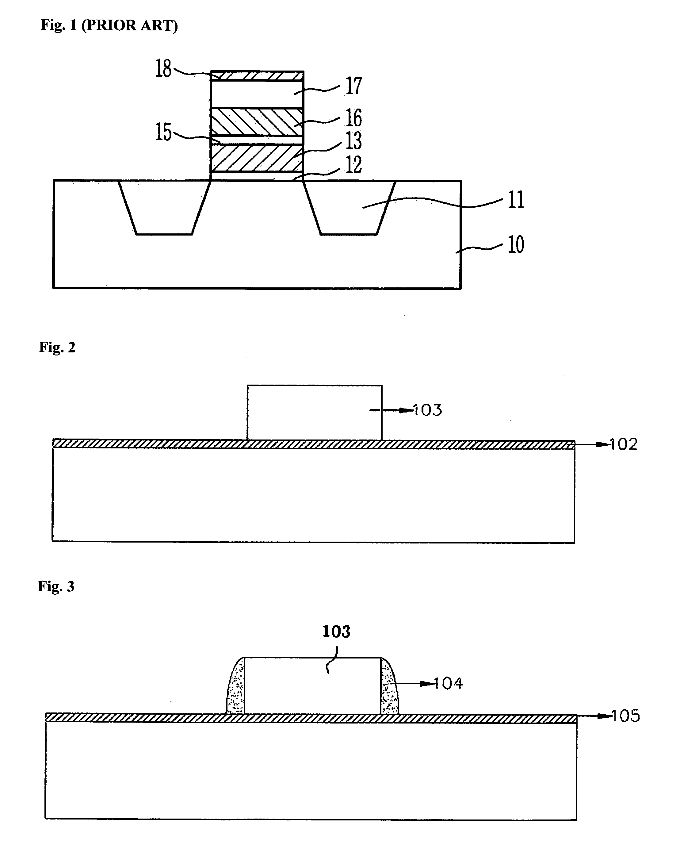
[0030] Referring to FIG. 2, a pad oxide layer 102 is grown on a p-type silicon substrate 101. Subsequently, a nitride layer 103 is deposited on the pad oxide layer 102. After a mask pattern for a drain region is formed on the nitride layer 103, the nitride layer 103 is etched by using the mask pattern. The nitride layer 103 can be replaced with an oxide layer or other insulating layers. In addition, the nitride layer 103 preferably has a thickness between 500 Å and 2500 Å.

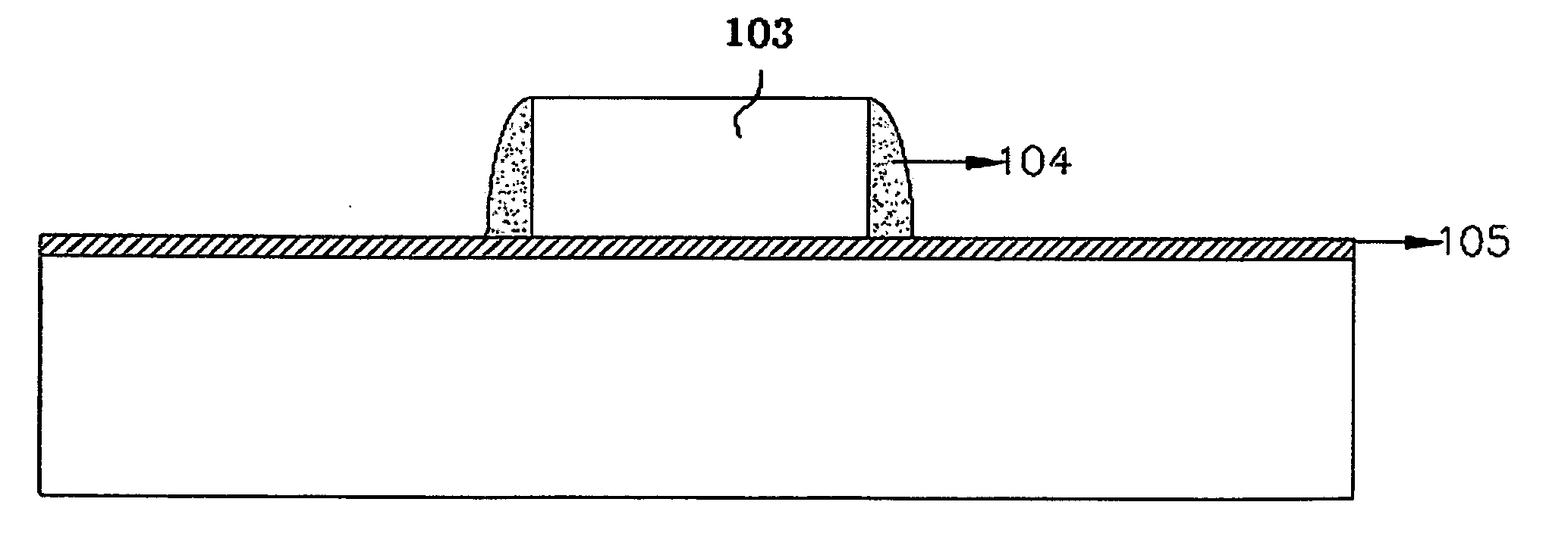
[0031] Referring to FIG. 3, the pad oxide layer 102 is removed except the area under the nitride layer 103. Subsequently, a tunnel oxide layer 105 is grown throug...


PUM


Abstract

Nonvolatile memory devices and methods of fabricating and driving the same are disclosed. Disclosed devices and method comprises: growing an oxide layer on a substrate and depositing a nitride layer on the oxide layer; patterning the nitride layer; forming injection gates on the lateral faces of the nitride layer; depositing a first polysilicon, a dielectric layer and a second polysilicon on the surface of the resulting structure, sequentially; patterning the second polysilicon, the dielectric layer and the second polysilicon to form gate electrodes; removing the nitride layer between the injection gates; forming source and drain extension regions around each of the gate electrodes by performing an ion implantation process; forming sidewall spacers on the lateral faces of the gate electrodes; and forming source and drain regions in the substrate by performing an ion implantation process with the sidewall spacers as an ion implantation mask.

Description

FIELD OF THE INVENTION [0001] The present disclosure relates to a nonvolatile memory and, more particularly, to nonvolatile memory devices and methods of fabricating and driving the same. BACKGROUND [0002] Generally, semiconductor memory devices are divided into volatile memories and nonvolatile memories. The volatile memories, including chiefly random access memories (RAM) such as dynamic random access memories (DRAM) and static random access memories (SRM), retain their memory data when the power is turned on, but lose the stored data when the power is turned off. In contrast, the nonvolatile memories, including chiefly read only memories (ROM), retain their memory data even after the power is turned off. [0003] The nonvolatile memories may be subdivided into ROM, programmable ROM (PROM), erasable PROM (EPROM), and electrically erasable PROM (EEPROM). [0004] From the view point of process technology, the nonvolatile memories may be divided into a floating gate family and a metal i...

Claims


Application Information

Patent Timeline
IPC IPC(8): G11C16/04H01L21/8247H01L27/115H01L29/423
CPCG11C16/0416G11C16/0433H01L29/42324H01L27/11521H01L27/11524H01L27/115H10B69/00H10B41/35H10B41/30
Inventor JUNG, JIN HYO
Owner DONGBU ELECTRONICS CO LTD
Why Eureka
Try Eureka