Thin film balun

a balun and thin film technology, applied in the field of balun, can solve the problems of increasing the effective capacitance on the side of the unbalanced transmission line, the difficulty of chip-type baluns, and the increase of the capacitance generated between the electrodes of the capacitor and the unbalanced terminal

Active Publication Date: 2010-07-01
TDK CORPARATION
View PDF9 Cites 5 Cited by
  • Summary
  • Abstract
  • Description
  • Claims
  • Application Information

AI Technical Summary

Benefits of technology

[0019]In the present invention, since the C component (capacitor) connected to the ground terminal is provided in the area between the outer end of the unbalanced terminal and the outer end of the ground terminal, ...

Problems solved by technology

However, if the resonant frequency fr is increased to a high frequency due to the size and thickness reductions of the thin film balun as described above, it will be difficult chip type baluns such as the one disclosed in reference 1 to satisfy such a required specification.
It is expected that, due to the reduced distance between, for ...

Method used


Image

  • Thin film balun
  • Thin film balun
  • Thin film balun

Examples


embodiment 1

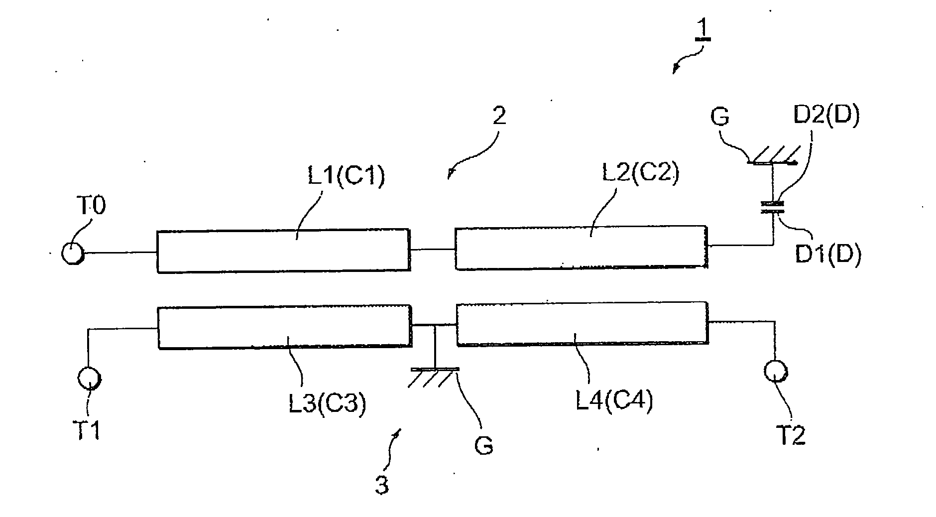
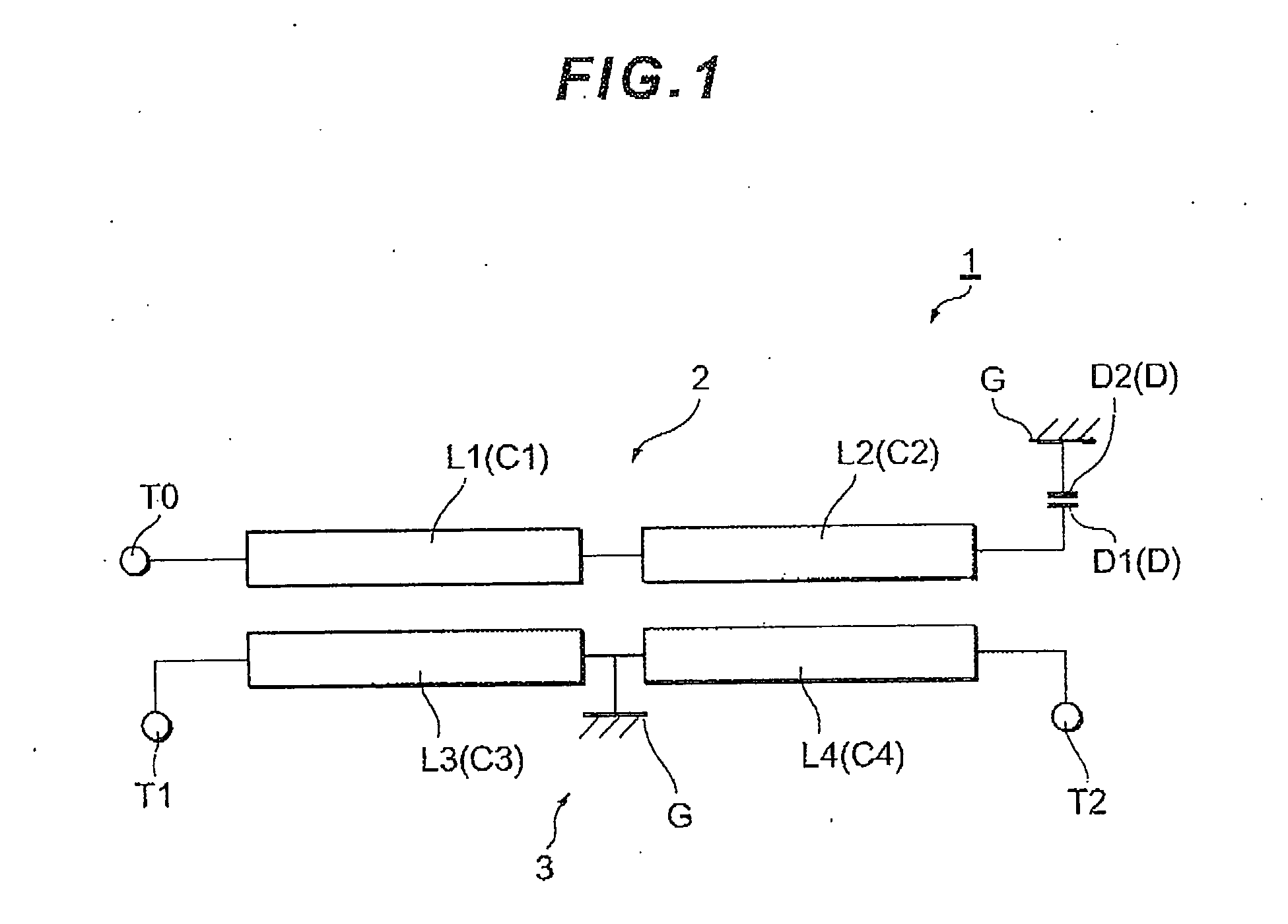
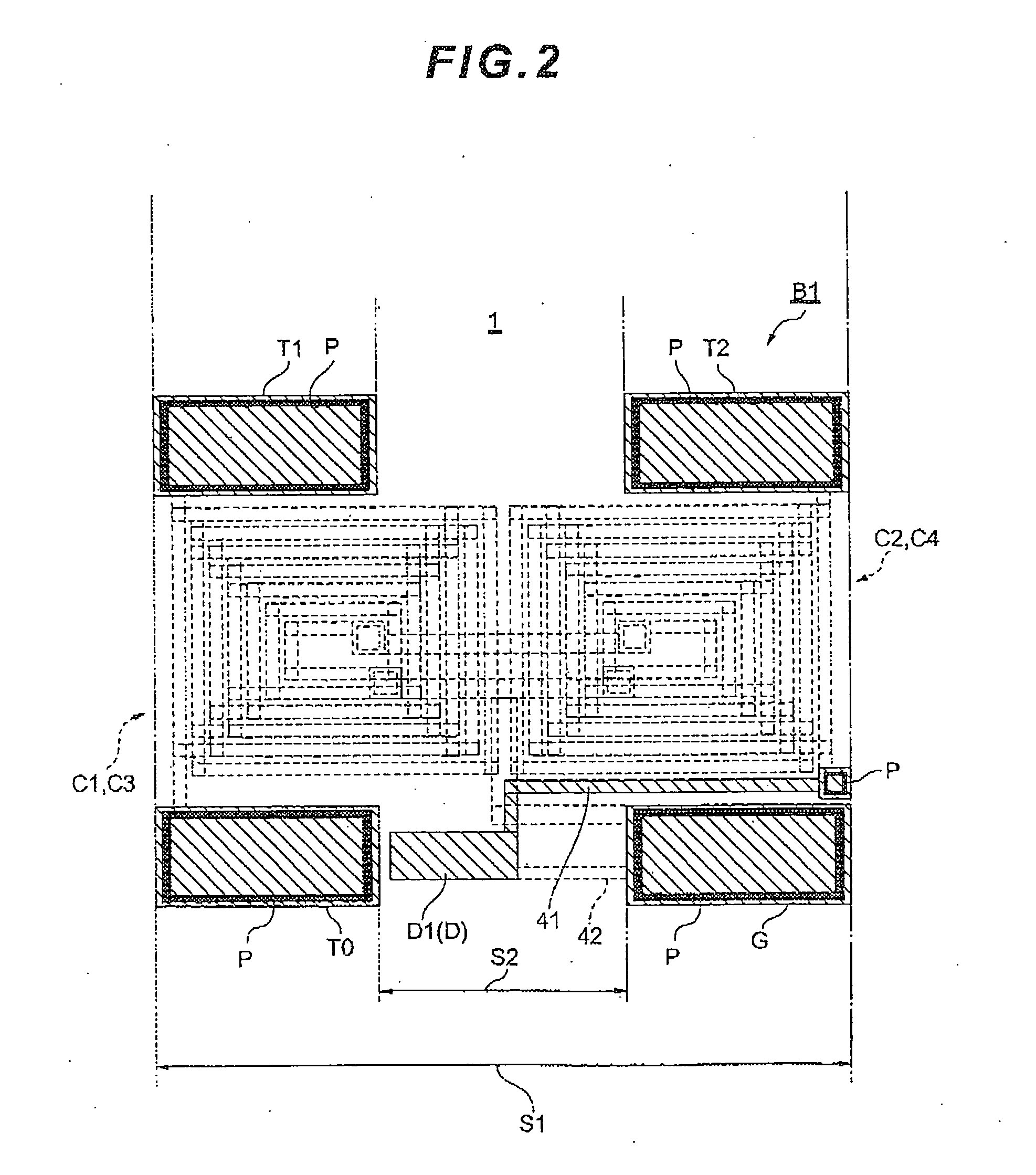
[0051]FIGS. 2 to 6 are horizontal sectional views schematically showing each wiring layer of the thin film balun 1 in embodiment 1. Specifically, FIG. 2 shows a horizontal cross section at a wiring layer B1 which is formed on an insulating substrate made of, for example, alumina. FIG. 3 shows a horizontal cross section at a wiring layer M0 formed in an insulating layer made of, for example, a polyimide (the same applies to insulating layers mentioned below) via a dielectric layer made of, for example, SiN. FIGS. 4 to 6 show respective horizontal cross sections at wiring layers M1, M2 and M3 which are sequentially formed above the wiring layer M0 respectively via insulating layers. As described above, the thin film balun 1 is constituted from thin film multiple wiring layers which are formed on the insulating substrate.

[0052]As shown in FIGS. 2 to 6, the unbalanced terminal T0, the balanced terminals T1 and T2, and the ground terminal G are formed on all of the wiring layers B1 and M...

embodiments 2a to 2k

[0060]FIGS. 7 to 17 are horizontal sectional views schematically showing wiring layers B1 in thin film baluns 2A to 2K in embodiments 2A to 2K according to the present invention. As shown in each figure, in the thin film baluns 2A to 2K, the entire capacitor D is arranged, in a plan view, in the above-described area S1 between the outer end of the unbalanced terminal T0 and the outer end of the ground terminal G, and in an area which overlaps with the coil portions C1 and C3 or overlaps with the coil portions C2 and C4 (i.e., the area outside the area S2). In the thin film baluns 2B, 2D and 21 of the thin film baluns 2A to 2K, the entire capacitor D is arranged, in a plan view, in the area S2 between the inner end of the unbalanced terminal T0 and the inner end of the ground terminal G. Note that, although only the electrode D1 of the capacitor D is shown in each of the figures, the electrode D2 having the same shape as that of the electrode D1 is formed at a position facing the ele...

embodiments 3a to 3c

[0061]FIGS. 18 to 20 are horizontal sectional views schematically showing wiring layers B1 in thin film baluns 3A to 3C in embodiments 3A to 3C according to the present invention. As shown in each figure, in the thin film baluns 3A to 3C, the entire capacitor D is arranged, in a plan view, in the area S2 between the inner end of the unbalanced terminal T0 and the inner end of the ground terminal G, the capacitor D spanning a first magnetic coupling area formed by the coil portions C1 and C3 and a second magnetic coupling area formed by the coil portions C2 and C4. Note that, although only the electrode D1 of the capacitor D is shown in each of the figures, the electrode D2 having the same shape as that of the electrode D1 is formed at a position facing the electrode D1 in the wiring layer M0.

[0062]COMPARATIVE EXAMPLE

[0063]FIG. 21 is a horizontal sectional view schematically showing a wiring layer B1 in a thin film balun 4 according to a comparative example. As shown in FIG. 21, in t...


PUM


Abstract

The present invention provides a thin film balun capable of preventing a resonant frequency from being increased to a high frequency, and thus realizing a preferable passage characteristic. A thin film balun 1 includes: an unbalanced transmission line 2 having a first coil portion C1 and a second coil portion C2; and a balanced transmission line 3 having a third coil portion C3 and a fourth coil portion C4 which are magnetically coupled with the first coil portion C1 and the second coil portion C2, respectively. The first coil portion C1 is connected to an unbalanced terminal T0, and the second coil portion C2 is connected to a ground terminal G (ground potential) via a capacitor D (C component). The third coil portion C3 is connected to a balanced terminal T1 and the fourth coil portion C4 is connected to a second balanced terminal T2. The capacitor D is provided, in a plan view, in an area S1 between the outer end of the unbalanced terminal T0 and the outer end of the ground terminal G.

Description

BACKGROUND[0001]1. Field of the Invention[0002]The present invention relates to a balun (a balun transformer) that performs conversion between unbalanced and balanced signals, and in particular relates to a thin film balun that is formed by a thin film process advantageous for size and thickness reductions.[0003]2. Description of Related Art[0004]A wireless communication device includes various high frequency elements such as an antenna, a filter, an RF switch, a power amplifier, an RF-IC, and a balun. Of these elements, a resonant element such as an antenna or a filter handles (transmits) an unbalanced signal which is based on a ground potential, whereas an RF-IC which generates or processes a high frequency signal handles (transmits) a balanced signal. Accordingly, when electromagnetically connecting these two elements, a balun that functions as an unbalanced-balanced converter is used.[0005]Recently, thin film baluns that are formed by a thin film process advantageous for size an...

Claims


Application Information

Patent Timeline
IPC IPC(8): H03H7/42
CPCH01F17/0006H01P5/10
Inventor ENDO, MAKOTO
Owner TDK CORPARATION
Why Eureka
Try Eureka