Read/Write Margin Improvement in SRAM Design Using Dual-Gate Transistors

a dual-gate transistor and read/write margin technology, applied in the field of integrated circuits, can solve problems such as errors in respective read and write operations, erroneous flip of sram cells, and above-discussed structures, and achieve the effects of improving read disturbance immunity, improving write ability, and low leakage curren

Inactive Publication Date: 2010-07-01
TAIWAN SEMICON MFG CO LTD
View PDF25 Cites 8 Cited by
  • Summary
  • Abstract
  • Description
  • Claims
  • Application Information

AI Technical Summary

Benefits of technology

[0009]The advantageous features of the present invention include reliable SRAM cells having improved write ability, low leakage currents during sleep mode operations, and improved immunity to read disturbance. In addition, substantially no chip-area penalty is incurred.

Problems solved by technology

Due to the existence of static noise, the reduced read and write margins may cause errors in the respective read and write operations.
The above-discussed structure, however, suffers from drawbacks.
This may cause an erroneous flip of SRAM cell 200.
An additional problem of the convention structure is that SRAM cells 100 and 200 may need to be laid out in such a way that the P-well or N-well regions have zigzag patterns, which adversely affect the scalability of the respective SRAM cells.

Method used


Image

  • Read/Write Margin Improvement in SRAM Design Using Dual-Gate Transistors
  • Read/Write Margin Improvement in SRAM Design Using Dual-Gate Transistors
  • Read/Write Margin Improvement in SRAM Design Using Dual-Gate Transistors

Examples


Embodiment Construction

[0016]The making and using of the embodiments of the present invention are discussed in detail below. It should be appreciated, however, that the embodiments of the present invention provide many applicable inventive concepts that can be embodied in a wide variety of specific contexts. The specific embodiments discussed are merely illustrative of specific ways to make and use the invention, and do not limit the scope of the invention.

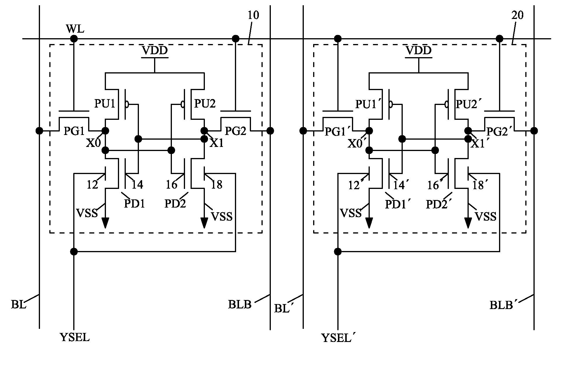
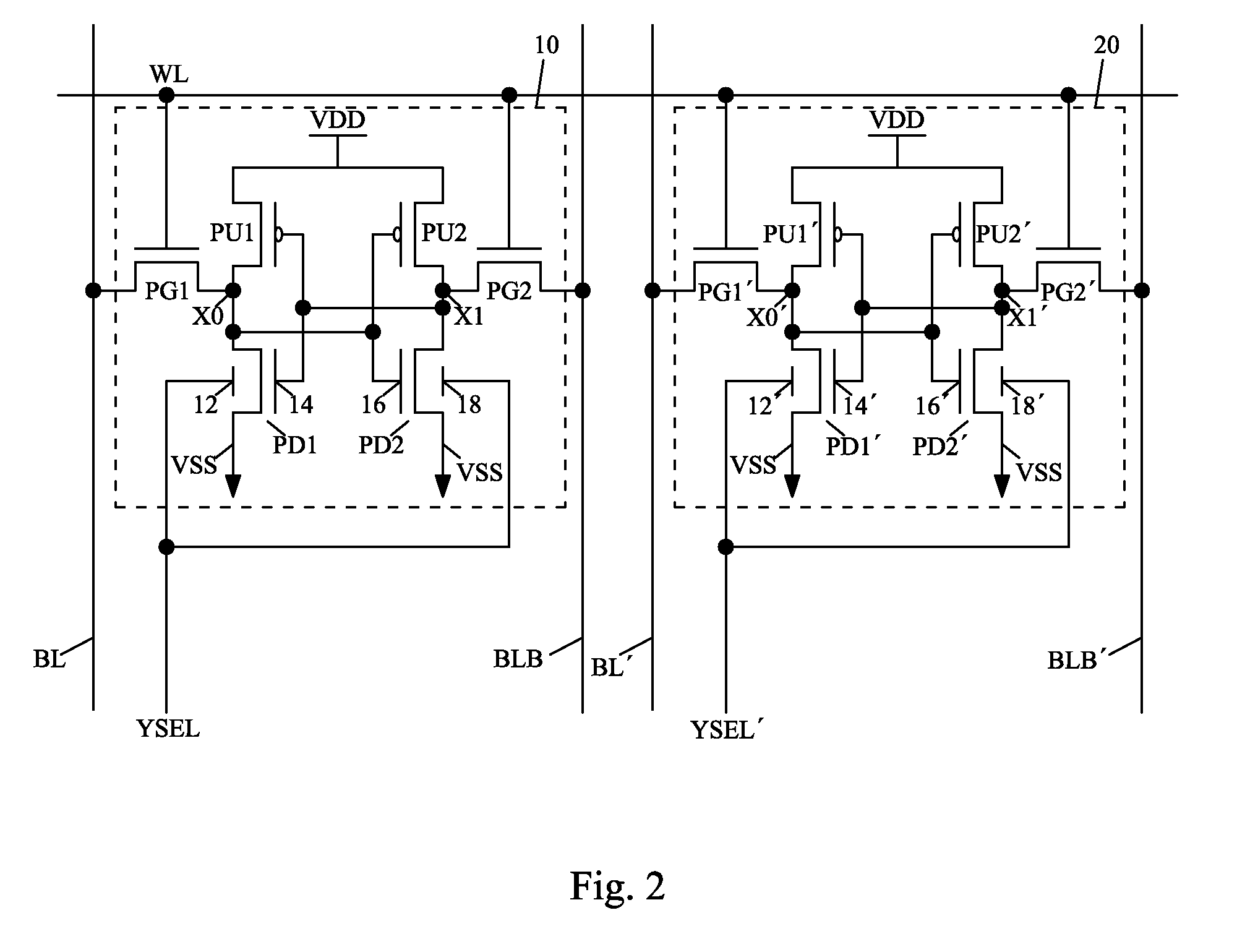
[0017]A novel static random access memory (SRAM) cell embodiment is provided. The variations and operation of the embodiment are discussed. Throughout the various views and illustrative embodiments of the present invention, like reference numbers are used to designate like elements.

[0018]FIG. 2 illustrates an embodiment of the present invention, which includes six-transistor (6-T) SRAM cells 10 and 20. SRAM cell 10 includes pull-up transistors (PMOS transistors) PU1 and PU2, pull-down transistors (NMOS transistors) PD1 and PD2, and pass-gate transistor ...


PUM


Abstract

An integrated circuit structure includes a static random access memory (SRAM) cell. The SRAM cell includes a pull-up transistor and a pull-down transistor forming an inverter with the pull-up transistor. The pull-down transistor includes a front gate connected to a gate of the pull-up transistor, and a back-gate decoupled from the front gate.

Description

TECHNICAL FIELD[0001]This invention relates generally to integrated circuits, and more particularly to memory cell design, and even more particularly to the structure and operations of static random access memory (SRAM) cells.BACKGROUND[0002]Static random access memory (SRAM) is commonly used in integrated circuits. SRAM cells have the advantageous feature of holding data without a need for refreshing. SRAM cells may include different numbers of transistors, and are often accordingly referred to by the number of transistors, for example, six-transistor (6-T) SRAM, eight-transistor (8-T) SRAM, and the like. The transistors typically form a data latch for storing a bit. Additional transistors may be added to control access to the transistors. SRAM cells are typically arranged as an array having rows and columns. Typically, each row of the SRAM cells is connected to a word-line, which determines whether the current SRAM cell is selected or not. Each column of the SRAM cells is connecte...

Claims


Application Information

Patent Timeline
Patent Type & Authority Applications(United States)
IPC IPC(8): G11C11/00G11C7/00
CPCG11C11/412H01L27/0207H01L27/11H01L27/1104H01L29/785H01L29/7855H10B10/00H10B10/12
Inventor CHEN, YEN-HUEIWU, JUI-JEN
Owner TAIWAN SEMICON MFG CO LTD
Why Eureka
Try Eureka