Microarray chip and method of fabricating for the same

a microarray and chip technology, applied in the field of microarray chips, can solve the problems of poor adhesion of resist material currently used in the preparation of microarray systems, inability to provide reliable experimental results, and the inability to conduct assays using such a microarray system

Inactive Publication Date: 2010-07-01
NAT INST OF HEALTH REPRESENTED BY THE SEC OF THE DEPT OF HEALTH & HUMAN SERVICES NAT INST OF HEALTH
View PDF4 Cites 61 Cited by
  • Summary
  • Abstract
  • Description
  • Claims
  • Application Information

AI Technical Summary

Benefits of technology

[0008]The present invention is directed to a microarray for use in the analysis of a sample and methods for preparing such microarrays. In particular aspects of the invention, the microarrays comprise a substrate covered with a coating material such as a commercially available photoresist film that has been patterned to form a plurality of microstructures on the substrate. The microarrays of the invention find particular use in high-throughput screening assays.

Problems solved by technology

The resist material currently used in the preparation of microarray systems, however, exhibits poor adhesion to a glass surface.
As a result, the resist material may peel off from a glass slide when the slide is immersed in the cell culture medium, and therefore, the cell-based assay conducted using such a microarray system may not provide reliable experimental results.

Method used


Image

  • Microarray chip and method of fabricating for the same
  • Microarray chip and method of fabricating for the same
  • Microarray chip and method of fabricating for the same

Examples


example 1

Array Chip Fabrication Using a Quartz Wafer

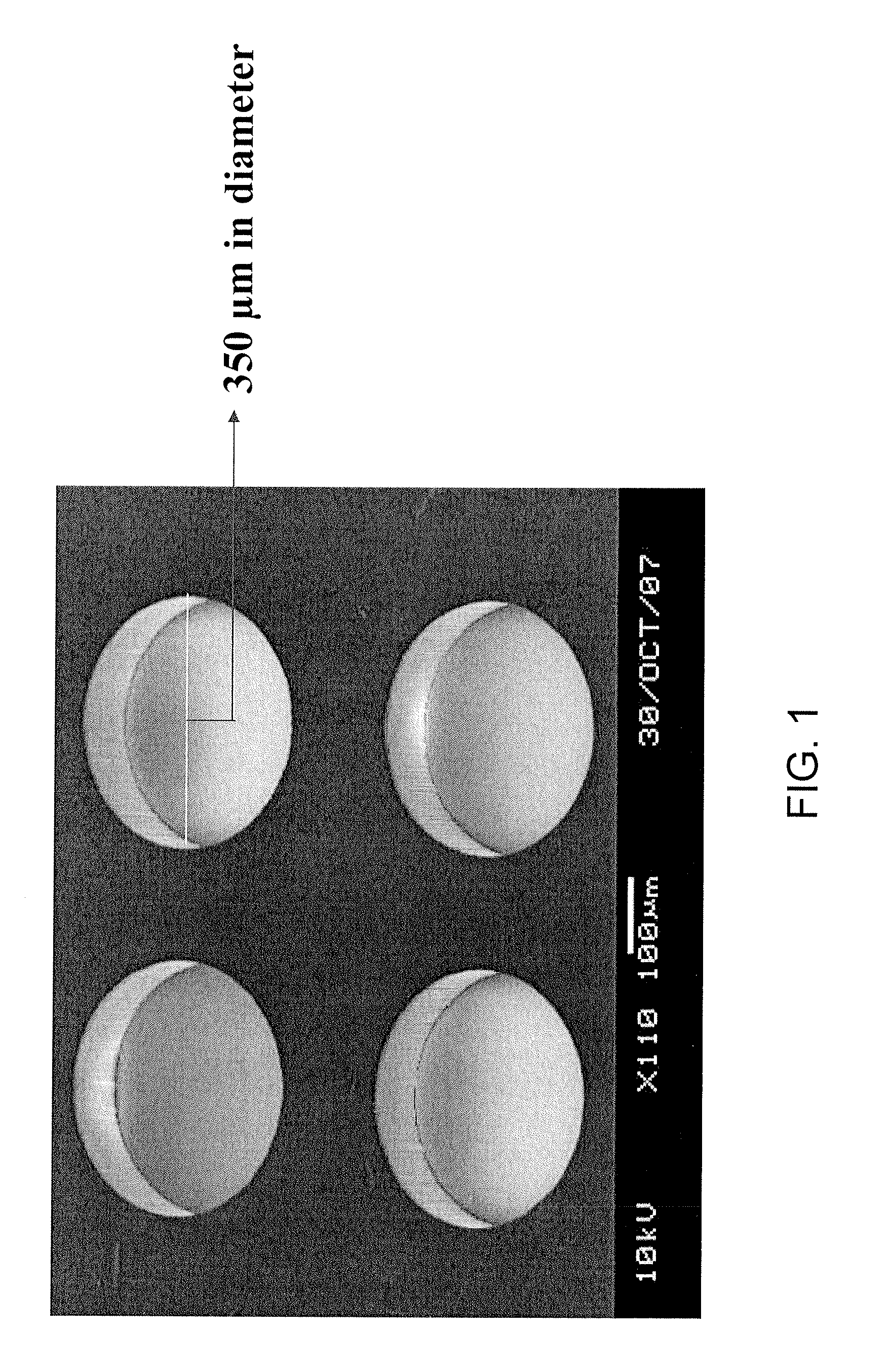
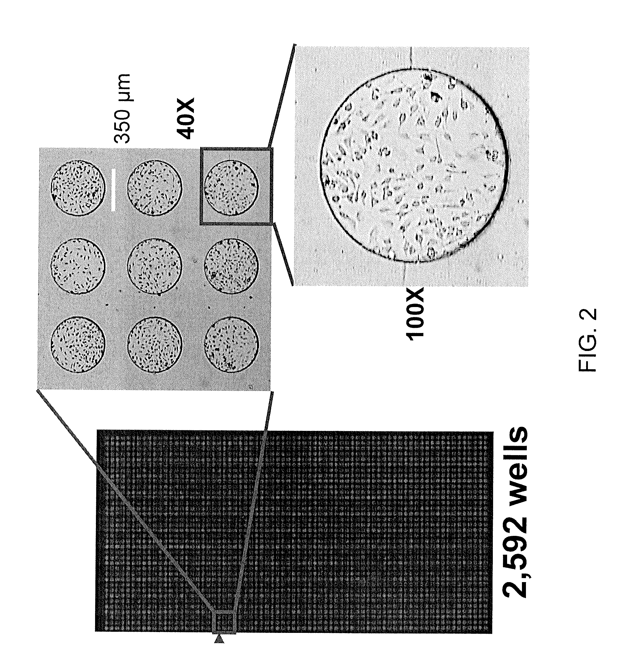
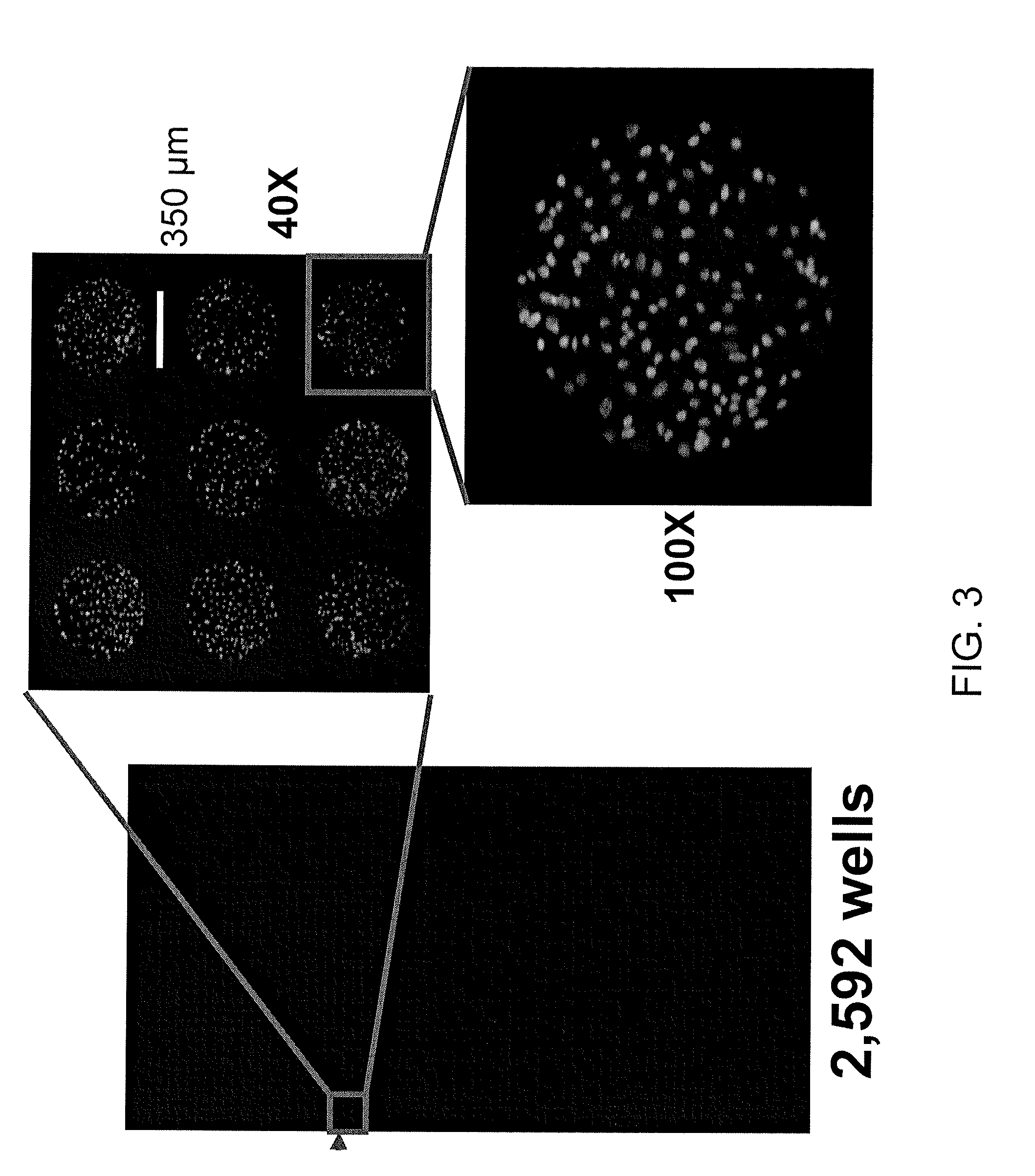
[0072]Quartz wafer was cleaned according to a Piranha Clean procedure as suggested (http: / / engineering.tufts.edu / microfab / index_files / SOP / PiranhaClean_SOP.pdf), and dried prior to coating with the photoresist material. The quartz wafer was then placed on a TEFLON™ carrier and submerged in a bath of 96% H2SO4:30% H2O2 solution (1:1) for 10-20 minutes to remove all organics. Next, the quartz wafer was removed from the bath and rinsed in deionized (DI) water for 15 minute. After the Piranha clean, the quartz wafer was blown dry with nitrogen or dried in an oven at 120° C. or on a hotplate at 150° C. and placed in a carrier box until ready for coating.

[0073]Commercially available photoresist material such as SU-8 100 film (MicroChem, Newton Mass.) having a thickness of about of 100 μm was spin-coated on the quartz wafer according to the coating conditions described as follow. During a spread cycle the wafer was ramped to 500 rpm at an accelerat...

example 2

Array Chip Fabrication Using a Glass Wafer

[0075]Glass wafer was cleaned by a Piranha clean procedure as described above and dried prior to coating with the photoresist. The glass wafer was then placed on a TEFLON™ carrier and submerged in a bath of H2O:H2O2:NH4OH solution (5:1:1) for 10 minutes. Next, the glass wafer was removed from the bath and rinsed in deionized (DI) water for 1 minute. The glass wafer was further submerged in a bath of H2O:HF solution (50:1) for 15 seconds and rinsed in the DI water for 1 minute. The glass wafer was submerged in a bath of H2O:H2O2:HCl solution (6:1:1) for 10 minutes and rinsed in DI water for 1 minute. After the RCA clean, the glass wafer was blown dry with nitrogen and placed in a carrier box until ready for coating.

[0076]Commercially available photoresist such as SU-8 3050 film (MicroChem, Newton Mass.) having a thickness of about 100 μm was spin-coated on a glass wafer according to the coating conditions described as follow. During a spread ...

example 3

Array Chip Fabrication Using a Silicon Wafer

[0078]Silicon wafer was cleaned by a Piranha clean procedure as described above and dried prior to coating with the photoresist. The silicon wafer was then placed on a TEFLON™ carrier and submerged in a bath of H2O:H2O2:NH4OH solution (5:1:1) for 10 minutes. Next, the silicon wafer was removed from the bath and rinsed in deionized (DI) water for 1 minute. The silicon wafer was further submerged in a bath of H2O:HF solution (50:1) for 15 seconds and rinsed in the DI water for 1 minute. The silicon wafer was submerged in a bath of H2O:H2O2:HCl solution (6:1:1) for 10 minutes and rinsed in DI water for 1 minute. After the Piranha clean, the silicon wafer was blown dry with nitrogen and placed in a carrier box until ready for coating.

[0079]Commercially available negative tone photoresist such as SU-8 50 film (MicroChem, Newton Mass.) having a thickness of about 50 μm was spin-coated on a glass wafer according to the coating conditions describe...


PUM

PropertyMeasurementUnit
thicknessaaaaaaaaaa
diameteraaaaaaaaaa
thicknessaaaaaaaaaa

Abstract

The present invention provides a microarray chip for use in the analysis of various sample types. The microarray chips disclosed herein generally comprise a substrate covered with a coating material comprising a photoresist material, wherein the coating material is patterned to comprise a plurality of microstructures such as microwells and/or microcolumns. Methods for preparing and utilizing the microarray chips of the invention are further provided. The microarray chips of the instant invention find particular use in high-throughput assays.

Description

CROSS-REFERENCE TO RELATED APPLICATIONS[0001]This application claims the benefit of U.S. Provisional Application No. 61 / 141,796, filed Dec. 31, 2008, which is hereby incorporated herein in its entirety by reference.BACKGROUND OF THE INVENTION[0002]The present invention relates to the fields of inorganic chemistry, organic chemistry, molecular biology, cellular biology, biochemistry and medicine. More particularly, the instant application discloses a microarray chip for analyzing a sample and method of fabricating for such microarray chips.[0003]Cell-based assays have long been used in cell research to understand basic mechanisms of cellular fate and function. Automated multiwell formats are one of the most widely used high-throughput screening systems. The current trend in plate-based screening systems is to reduce the volume of the reaction wells further, thereby increasing the density of the wells per plate. The reduction in reaction volumes results in increased throughput, dramat...

Claims


Application Information

Patent Timeline
Patent Type & Authority Applications(United States)
IPC IPC(8): C40B30/04C40B40/00C40B60/12
CPCB01J2219/00317B01J2219/00509B01J2219/0072B01J2219/00743B01L3/5085B01L2300/0636B01L2300/0819B01L2300/0829G01N33/5008
Inventor JUANG, JYH-LYHHUANG, YI-YOUCHEN, PO-CHENG
Owner NAT INST OF HEALTH REPRESENTED BY THE SEC OF THE DEPT OF HEALTH & HUMAN SERVICES NAT INST OF HEALTH
Why Eureka
Try Eureka