Liquid crystal display device and manufacturing method thereof

a liquid crystal display and manufacturing method technology, applied in non-linear optics, instruments, optics, etc., can solve the problems of reducing the yield rate of reflective liquid crystal display devices, difficulty in removing foreign materials, and minute cracks, so as to reduce the probability of foreign materials at the time of adhering the upper polarizer to the counter substrate, the effect of increasing the thickness of liquid crystal display devices

Inactive Publication Date: 2010-07-08
PANASONIC LIQUID CRYSTAL DISPLAY CO LTD +1
View PDF0 Cites 10 Cited by
  • Summary
  • Abstract
  • Description
  • Claims
  • Application Information

AI Technical Summary

Benefits of technology

[0018]According to the present invention, in the TFT substrate, the portions of the TFT substrate to which the lower polarizer is adhered are made thin by chemical polishing while allowing the peripheral portions of the TFT substrate to maintain the large thickness. Further, three peripheral sides of the counter substrate are formed into the U-shaped thick portion and one peripheral portion of the counter substrate which corresponds to the terminal portion and the portion of the counter substrate to which the upper polarizer is adhered are made thin by chemical polishing. Accordingly, it is possible to decrease the thickness

Problems solved by technology

Accordingly, when a foreign material is present in the recessed portion, it is difficult to remove the foreign material.
When the polarizer is adhered to the glass substrate in a state where the foreign material is present in the recessed portion, portions where the foreign material is present bring about screen defects thus lowering a yield rate of the reflective liquid crystal display device.
In such a dividing method, there may be a possibility that minute cracks occur

Method used


Image

  • Liquid crystal display device and manufacturing method thereof
  • Liquid crystal display device and manufacturing method thereof
  • Liquid crystal display device and manufacturing method thereof

Examples


embodiment 1

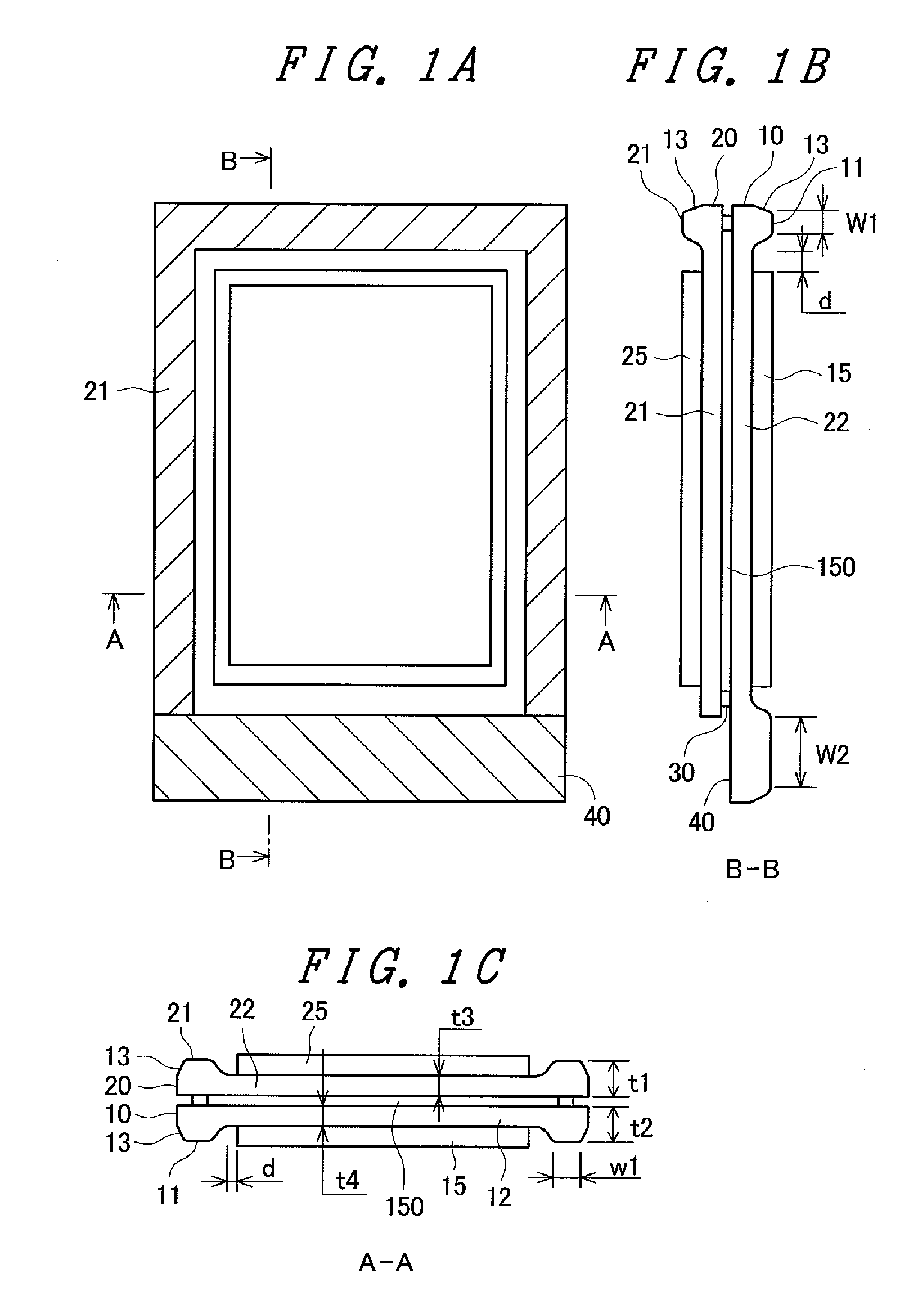
[0030]FIG. 1A to FIG. 10 show an example of a liquid crystal display device to which the present invention is applied. FIG. 1A to FIG. 1C shows a case where the liquid crystal display device is used in a mobile phone or the like. FIG. 1A is a plan view of the liquid crystal display device, FIG. 1B is a cross-sectional view of the liquid crystal display device taken along a line B-B in FIG. 1A, and FIG. 10 is a cross-sectional view of the liquid crystal display device taken along a line A-A in FIG. 1A.

[0031]In FIG. 1A, a counter substrate 20 is arranged on a TFT substrate 10. The TFT substrate 10 and the counter substrate 20 are adhered to each other by a sealing material 30 shown in FIG. 1B which is formed on peripheries of respective substrates. A liquid crystal layer 150 shown in FIG. 1B is sandwiched between the TFT substrate 10 and the counter substrate 20, and the liquid crystal layer 150 is sealed with the sealing material 30.

[0032]In FIG. 1A, a counter-substrate thick portion...

embodiment 2

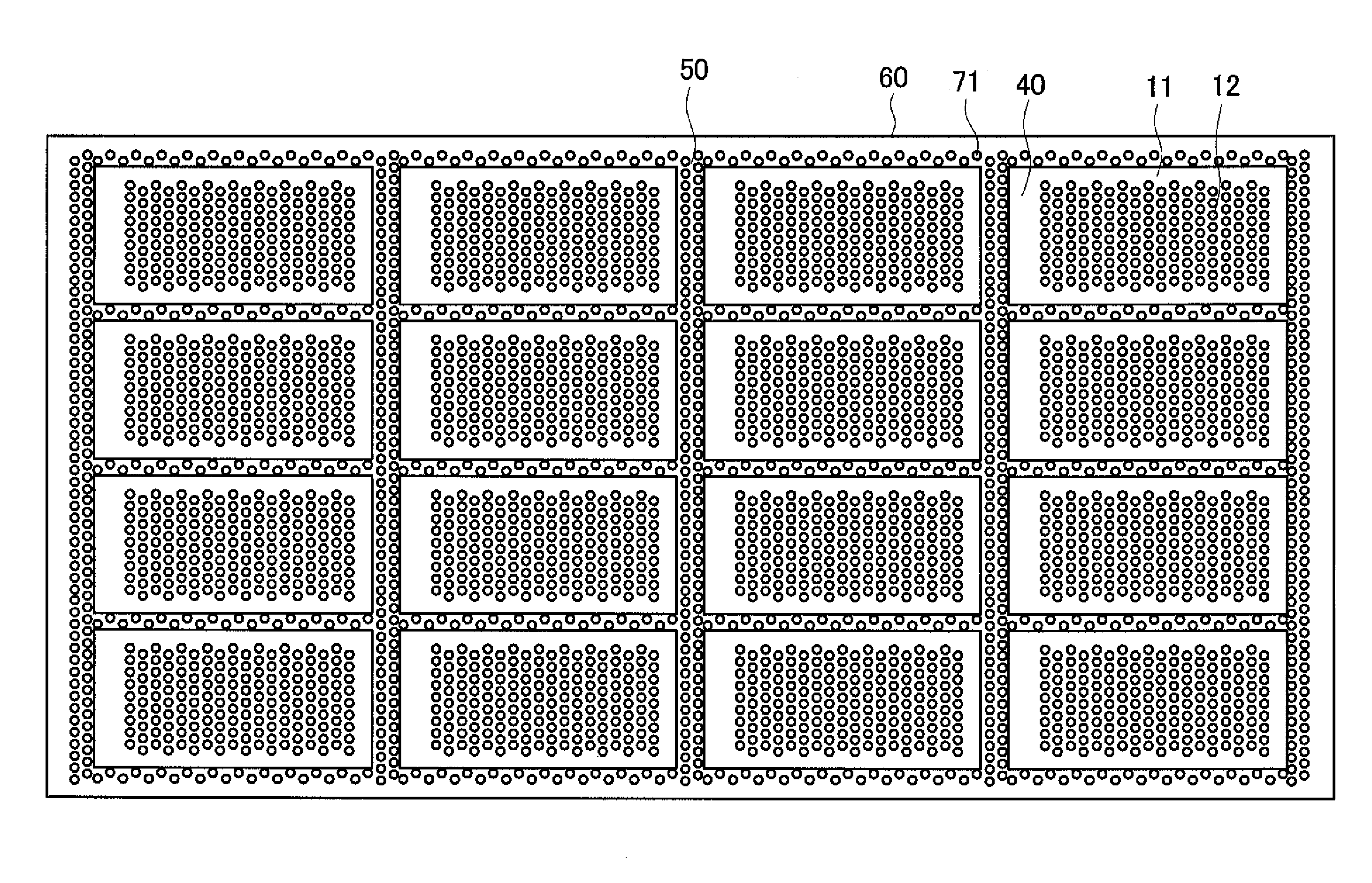
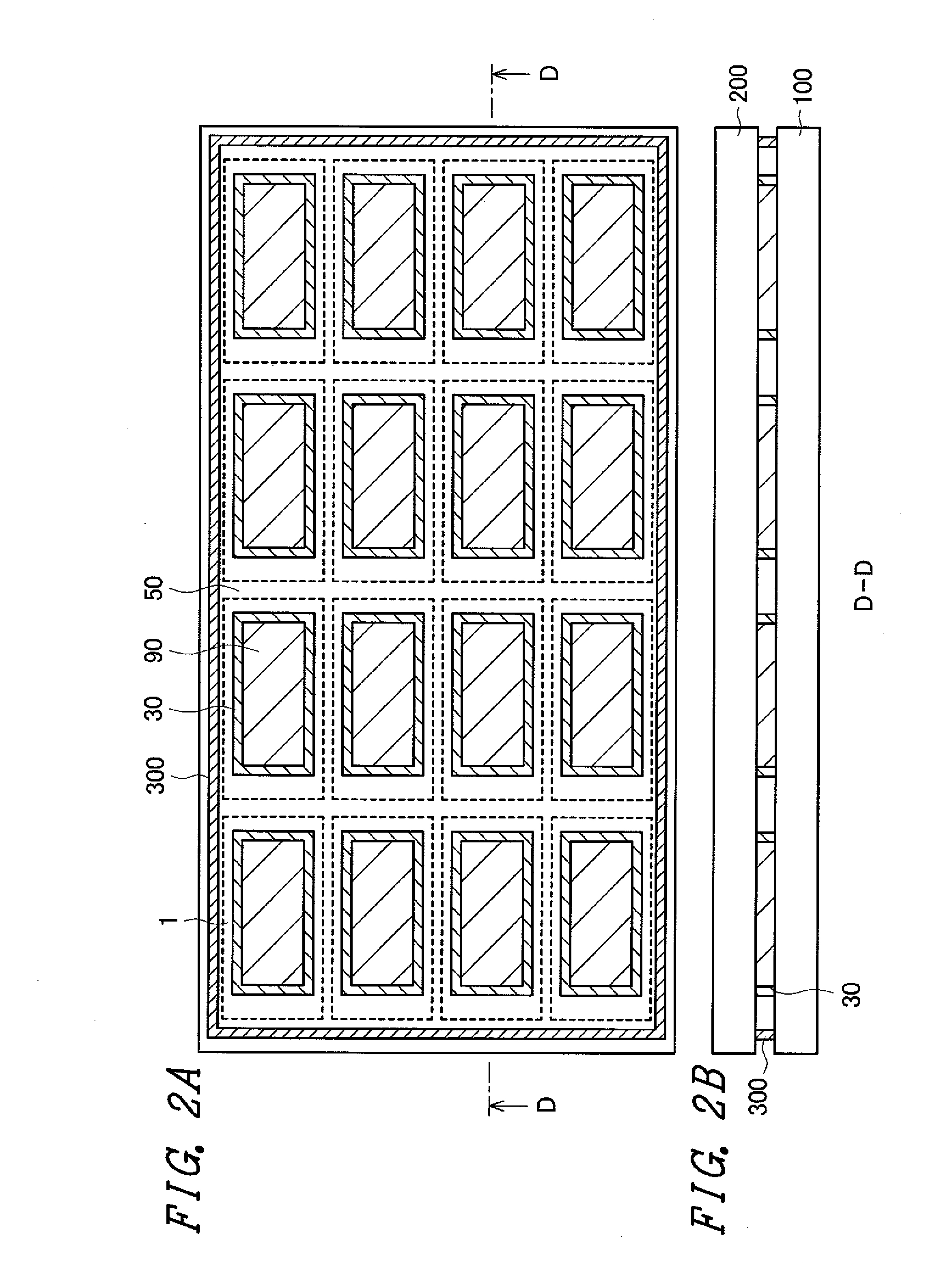
[0069]In the explanation of the embodiment 1, the explanation has been made with respect to the method in which the thick portion and the thin portion are formed on the TFT substrate 10 and the counter substrate 20 of the individual liquid crystal cell 1 respectively in the step of polishing the mother substrate. In the embodiment 1, the adhesion of the mask 60 becomes necessary for every individual liquid crystal cell 1. That is, for example, as shown in FIG. 3, when 16 pieces of TFT substrates 10 are formed on the mother TFT substrate 100, 16 pieces of masks 60 become necessary. Accordingly, 16 pieces of masks 60 are adhered for every one mother TFT substrate 100. Further, 16 pieces of masks 60 are adhered for every one mother counter substrate 200. As described above, there exists a possibility that the adhesion of a large number of masks 60 to the mother substrate lowers a throughput.

[0070]This embodiment provides a method in which a portion having a large thickness and a portio...

embodiment 3

[0075]FIG. 9 shows an example of a mask 60 for applying chemical polishing to a mother TFT substrate 100 in the embodiment 3 of the present invention. In FIG. 9, different from the embodiment 2, on portions of the mask 60 corresponding to portions of TFT substrates 10 to which an upper polarizer 25 is adhered, a window portion 65 is formed. On the other hand, in the same manner as the scribing regions 50 in the second embodiment, a large number of holes 71 are formed in portions of the mask 60 corresponding to the scribing regions 50.

[0076]In the embodiment 2, with respect to the TFT substrate 10, the portion of the TFT substrate 10 to which the upper polarizer 25 is adhered is also polished by chemical polishing using the mask 60 in a meshed shape where a large number of holes 71 are formed. When the chemical polishing is performed through the small holes 71, there may be a case where the portion of the TFT substrate 10 corresponding to the hole 71 is deeply etched, and the portion...


PUM


Abstract

In a miniaturized liquid crystal display device, a thickness of the liquid crystal display device is decreased and the occurrence of cracks is prevented. A portion of a TFT substrate to which a lower polarizer is adhered has a small thickness, and a periphery of the TFT substrate including a terminal portion has a large thickness. A portion of a counter substrate to which an upper polarizer is adhered has a small thickness, and a periphery of the counter substrate except for one side which forms a U shape has a large thickness. Accordingly, in adhering the upper polarizer to the counter substrate, it is possible to decrease a possibility that a foreign material is entangled. By applying chemical polishing to edge portions of the TFT substrate and edge portions of the counter substrate, the edge portions are rounded and hence, the probability of occurrence of cracks caused by an impact or the like from the outside can be decreased.

Description

CLAIM OF PRIORITY[0001]The present application claims priority from Japanese application serial No. 2009-1606, filed on Jan. 7, 2009, the content of which is hereby incorporated by reference into this application.BACKGROUND OF THE INVENTION[0002]1. Field of the Invention[0003]The present invention relates to a display device, and more particularly to a liquid crystal display device which can decrease a thickness thereof and can prevent chipping of an edge portion of a substrate.[0004]2. Description of the Related Art[0005]A liquid crystal display device includes a TFT substrate on which pixel electrodes, thin film transistors (TFT) and the like are formed in a matrix array, a counter substrate which faces the TFT substrate in an opposed manner and mounts color filters or the like thereon at positions corresponding to the pixel electrodes on the TFT substrate, and liquid crystal which is sandwiched between the TFT substrate and the counter substrate. In the liquid crystal display dev...

Claims


Application Information

Patent Timeline
IPC IPC(8): G02F1/1345G02F1/13
CPCG02F1/1333
Inventor SAITOU, KAZUNARIKOBARA, KATSUMIITAKURA, MASAHARU
Owner PANASONIC LIQUID CRYSTAL DISPLAY CO LTD
Why Eureka
Try Eureka