
RFID tag

a radio frequency identification and tag technology, applied in the field of rfid (radio frequency identification) tags, can solve the problems of increasing cost, complicated structure of rfid tags, and reducing the so as to prevent the shortened range in which rfid tags can carry out communications from being upsized , the effect of reducing the cross-polarization component and reducing the electric supply loss

Inactive Publication Date: 2010-07-22
MITSUBISHI ELECTRIC CORP
View PDF14 Cites 35 Cited by
  • Summary
  • Abstract
  • Description
  • Claims
  • Application Information

AI Technical Summary

Benefits of technology

The present invention provides an RFID tag that can be mounted on a curved surface with a predetermined curvature. The tag includes a dielectric substrate with a hole in its main surface, a ground conductive pattern, a conductive pattern on the inner portion of the substrate, and an IC chip electrically connected to the conductive pattern. The tag also includes a first dielectric substrate with a recessed portion and a second dielectric substrate with higher hardness than the first substrate. The technical effect of this invention is to provide an RFID tag that can be easily mounted on curved surfaces and provide reliable performance even at extreme temperatures.

Problems solved by technology

Because an active-type tag is equipped with a battery, it has merits in view of a communication range, communicative stability, etc., compared with a passive-type tag, while because an active-type tag has a complicated structure, it has demerits of being upsized, increasing in cost, and so on.
Therefore, although there is a low possibility that the IC chip is damaged by a shock or the like, a problem is that the structure of the RFID tag is complicated and the manufacture (mass production) of the RFID tag becomes difficult.
That is, a problem is that when mounting the antenna pattern and the IC chip on the base material, there is a possibility that the IC chip is damaged by a shock or the like, and it is therefore difficult to print a label directly on the front surface (the upper surface) of the RFID tag by using a label printer.
Furthermore, even in a case in which a film on which the antenna pattern and the IC chip are mounted is bonded onto the base material, the problem as mentioned above arises because a bulge (a projection) occurs in the film due to the mounting of the IC chip.
A problem with the RFID tag disclosed by patent reference 3 is that although a bulge (a projection) hardly occurs in the film (the film base) due to the mounting of the IC chip, in a case in which the RFID tag is attached to a conductive object (a conductor) such as a metal body or is mounted in a vicinity of a conductive object, the loop antenna stops operating under the influence of the conductive object, and the communication range drops extremely.
A problem with the RFID tag disclosed by patent reference 4 is that although a bulge (a projection) hardly occurs in the film due to the mounting of the IC chip, in a case in which the RFID tag is attached to a conductive object (a conductor) such as a metal body or is mounted in a vicinity of a conductive object, the loop antenna or dipole antenna stops operating under the influence of the conductive object, and the communication range drops extremely, as in the case of RFID tag disclosed by patent reference 3.
For this reason, as in the case of the RFID tag disclosed by patent reference 2, a problem is that there is a possibility that the IC chip is damaged by a shock or the like, and it is therefore difficult to print a label directly on the front surface (the upper surface) of the RFID tag by using a label printer.
Furthermore, in a case in which a film on which the antenna pattern and the IC chip are mounted is bonded onto the base material, the problem as mentioned above arises because a bulge (a projection) occurs in the film due to the mounting of the IC chip.
A further problem is that because the cross polarization component occurring is radiated in a direction different from the direction which is intended originally for the correct polarization, there is a case in which the tag communicates with the reader / writer even though the tag is placed at a location where the reader / writer does not desire to communicate with the tag, so that the implementation of the mounting method of mounting the tag and the managing method of managing the tag becomes difficult.
In addition, a problem with the patch antenna of the RFID tag disclosed by patent reference 5 is that although the feeding points 41 and 42 are located in a vicinity of the center of the antenna face 30, the pattern of the correct polarization wave also becomes asymmetrical and therefore affects the symmetry of the radiation pattern of the antenna because the patch antenna is based on the placement of the slit at a position shifted from the center of the antenna face 30.
In addition, a problem is that because a magnetic field occurs in a direction of the length of the slot shown in FIG. 1 of patent reference 5, and the RFID tag is resonated and radiates an electric wave with this length, the slot has to have a length of the order of about λ / 2 in order that the RFID tag radiates an electric wave with a high degree of efficiency, and the downsizing of the RFID tag becomes difficult.

Method used


Image

  • RFID tag
  • RFID tag
  • RFID tag

Examples


embodiment 1

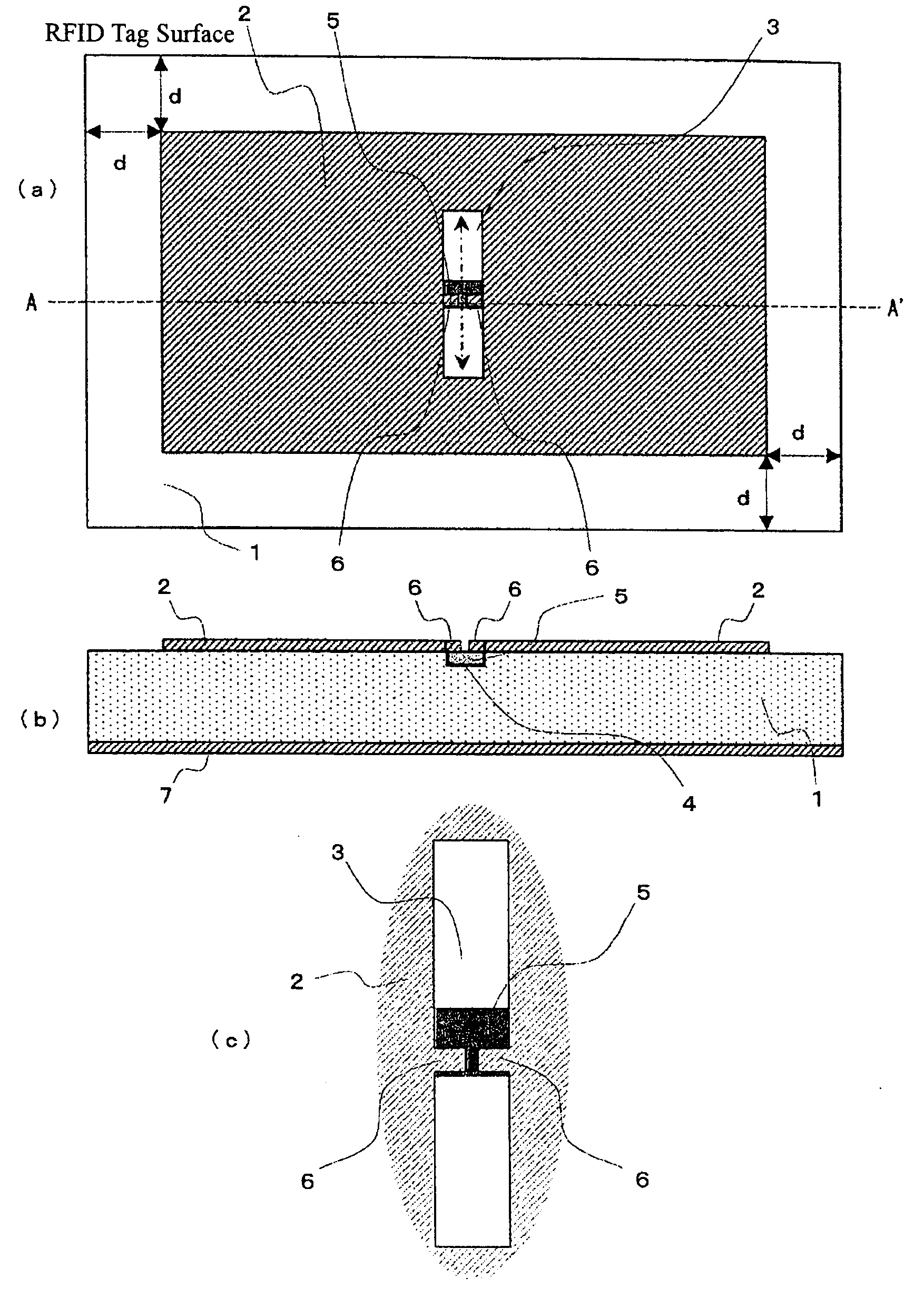
[0086]Embodiment 1 of the present invention will be explained hereafter. FIG. 1 is a configuration diagram of an RFID tag in accordance with this Embodiment 1. FIG. 1(a) is a plan view of the RFID tag, FIG. 1(b) is a cross-sectional view taken along the A-A′ line shown in FIG. 1(a), and FIG. 1(c) is a plan view showing an enlarged part in a vicinity of a slot of the RFID tag shown in FIG. 1(a). In these figures FIGS. 1(a) to 1(c), a conductive pattern 2 is disposed on one main surface (a front surface) of a dielectric substrate 1. As shown in FIG. 1(a), the conductive pattern 2 is formed in an inner portion of the dielectric substrate 1 in such a way as to be at a distance d from each of vertical edges and horizontal edges of the dielectric substrate 1. As shown in FIG. 1(a), a long narrow slot 3 is formed in a central portion of the conductive pattern 2. This slot 3 can be formed by making the conductive pattern 2 be subjected to an etching process, a milling process, vapor deposit...

embodiment 2

[0099]Embodiment 2 of the present invention will be explained with reference to FIG. 7. FIG. 7 is a plan view showing the structure of an RFID tag in accordance with Embodiment 2, FIG. 7(a) is a plan view of the RFID tag, and FIG. 7(b) is a plan view showing an enlarged part in a vicinity of a slot of the RFID tag shown in FIG. 7(a). In the figures, the same reference numerals denote the same components or like components, and therefore the detailed explanation about them will be omitted hereafter. In Embodiment 1, the case in which the number of terminals (not shown) of the IC chip 5 is two, i.e., the IC chip having two legs is used is explained. In contrast, in this embodiment, an IC chip 5 having four terminals is mounted, and, in addition to electrical connecting portions 6 and 6 as explained in Embodiment 1, two dummy pads 23 and 23 are disposed inside the slot 3 in a vicinity of the electrical connecting portions 6 and 6. In a formation method of forming these dummy pads 23 an...

embodiment 3

[0100]Embodiment 3 of the present invention will be explained with reference to FIGS. 8 to 10. FIG. 8 is a configuration diagram showing the structure of an RFID tag in accordance with Embodiment 3, FIG. 8(a) is a plan view of the RFID tag, FIG. 8(b) is an enlarged view of a slot of the RFID tag in accordance with Embodiment 3, FIG. 9 is a configuration diagram showing the structure of an RFID tag in accordance with Embodiment 3, and FIG. 10 is a configuration diagram showing the structure of an RFID tag in accordance with Embodiment 3. In FIGS. 8 to 10, a taper-shaped slot 24 is formed in such a way as to widen along each of opposing directions of its length with distance from the position at which an IC chip 5 is placed, and an electric length adjusting unit 25 is formed in each of edge portions of a conductive pattern 2 in such a way as to be shaped like a cutout portion. A slot 26 is formed in such a way as to have an angle with respect to the sides of a conductive pattern 2, an...


PUM


Abstract

An RFID tag characterized in including: a dielectric substrate having a hole formed in one main surface thereof; a ground conductive pattern disposed on another main surface of this dielectric substrate; a conductive pattern disposed on the one main surface of the above-mentioned dielectric substrate in such a way as to be placed in an inner portion of the dielectric substrate at a predetermined distance from each of edges of the above-mentioned dielectric substrate, a slot being formed in this conductive pattern; and an IC chip electrically connected to the above-mentioned conductive pattern via this slot, and inserted into the above-mentioned hole of the above-mentioned dielectric substrate.

Description

FIELD OF THE INVENTION [0001]The present invention relates to an RFID (Radio Frequency Identification) tag that receives a command signal transmitted from a reader / writer to update tag information stored in a memory thereof according to information shown by the command signal or additionally write information in the tag information, or transmits the tag information to the RFID reader / writer as a read signal, and that is used for entrance / exit control, physical distribution management, or the like of living bodies or products.BACKGROUND OF THE INVENTION[0002]An RFID system enables radio communications to be carried out between an RFID tag equipped with an IC chip and an RFID reader / writer. RFID tags include an active-type tag in which a battery is mounted and runs from the electric power of the battery, and a passive-type tag that receives electric power from a reader / writer and runs from this electric power. Because an active-type tag is equipped with a battery, it has merits in vie...

Claims


Application Information

Patent Timeline
Patent Type & Authority Applications(United States)
IPC IPC(8): G06K19/077G06K19/063
CPCG06K19/07749G06K19/07786H01Q13/106H01Q1/38H01Q1/2225
Inventor OKEGAWA, HIROKATSUENOMOTO, HIDEONOKAMI, YOHEIKANEKO, KIMIHIROIWAKURA, TAKASHIRYOKI, HIROFUMI
Owner MITSUBISHI ELECTRIC CORP
Learn More