Short path customized mask correction

Inactive Publication Date: 2010-07-22
GLOBALFOUNDRIES INC
View PDF17 Cites 17 Cited by
  • Summary
  • Abstract
  • Description
  • Claims
  • Application Information

AI Technical Summary

Benefits of technology

[0023]Embodiments of the present invention provide a method and a system for generating a set of photo-mask shapes that are capable of transferring design intent of semiconductor devices onto wafers with minimal design rule implication and impact on locally specialized artifacts that are applied globally, referred to as global solution. Embodiments of the present invention provide a way of addressing hot-spots in the design of photo-mask shapes, by applying a methodology of creating and using a library of pre-computed mask correction solutions, in the form of tagging solutions on the fly, to problem areas identified, correcting them in the best possible way known for the given problem, and integrating the solution into the final mask design. Embodiments of the present invention also provide a method of synchronizing design and simulation for optical lithography across different working entities, such as companies and / or organizations, optionally through a network, by implementing the method on a common service-oriented architecture (SOA).

Problems solved by technology

Today's semiconductor device manufacturing process has pushed resolution limits of certain tools and materials used in optical lithography to a point where catastrophic failures may occur for some configurations if not being designed carefully.
However, as geometries of device patterns continue to shrink, these design rules have often been found incapable of adequately safeguarding device patterns against all failure mechanisms.
In order to protect against design failure, attempts to modify currently existing design rules have led to design rules that are overly conservative and not competitive.
In the meantime, the creation of a new set of design rules that is sufficiently detailed and comprehensive to ensure manufacturability of all designs, yet being succinct and compact such that device designers may learn quickly and adhere to it, is becoming increasingly difficult.
However, this trend cannot continue as the amount of time required to create and introduce new design rules and the amount of knowledge required by individual designers is growing at a rate that clearly cannot be sustained.
However, due to the need for competitive design rules, which as a result may have pushed process margins to their extremes, the MDP process may fall short at times. Moreover, tight process margins may create patterns that are sensitive to details of the MDP process.
For example, failures may occur due to mask making constraints that inhibit some best mask artifacts and cause software limitations, and may occur due to locally inserted perturbation that was intended to correct a known problem, but adversely cause similar but not identical geometrical shapes to fail.
The reality may be made even more difficult by the process variations that affect preponderantly some small areas of design.
Here, it shall be noted that solutions specifically crafted for these cases are often, unfortunately, less than optimum for creating a robust mask and therefore the approach of crafting solutions is generally not considered as practical.
However, neither the DFM tool nor the designers have any knowledge of how each hot spot will be impacted by subsequent changes to the used MDP algorithm.
It shall be noted that even though above design process, as being illustrated in FIG. 1, may contain information of mask shapes that the designer intends to print on a wafer, information such as, e.g., conditions of the MDP process used in the DFM tool may not be properly recorded and may have been lost during the process.
Attaining a proper tradeoff between the two in the shortest possible development cycle remains a major challenge in the industry.

Method used


Image

  • Short path customized mask correction
  • Short path customized mask correction
  • Short path customized mask correction

Examples


Embodiment Construction

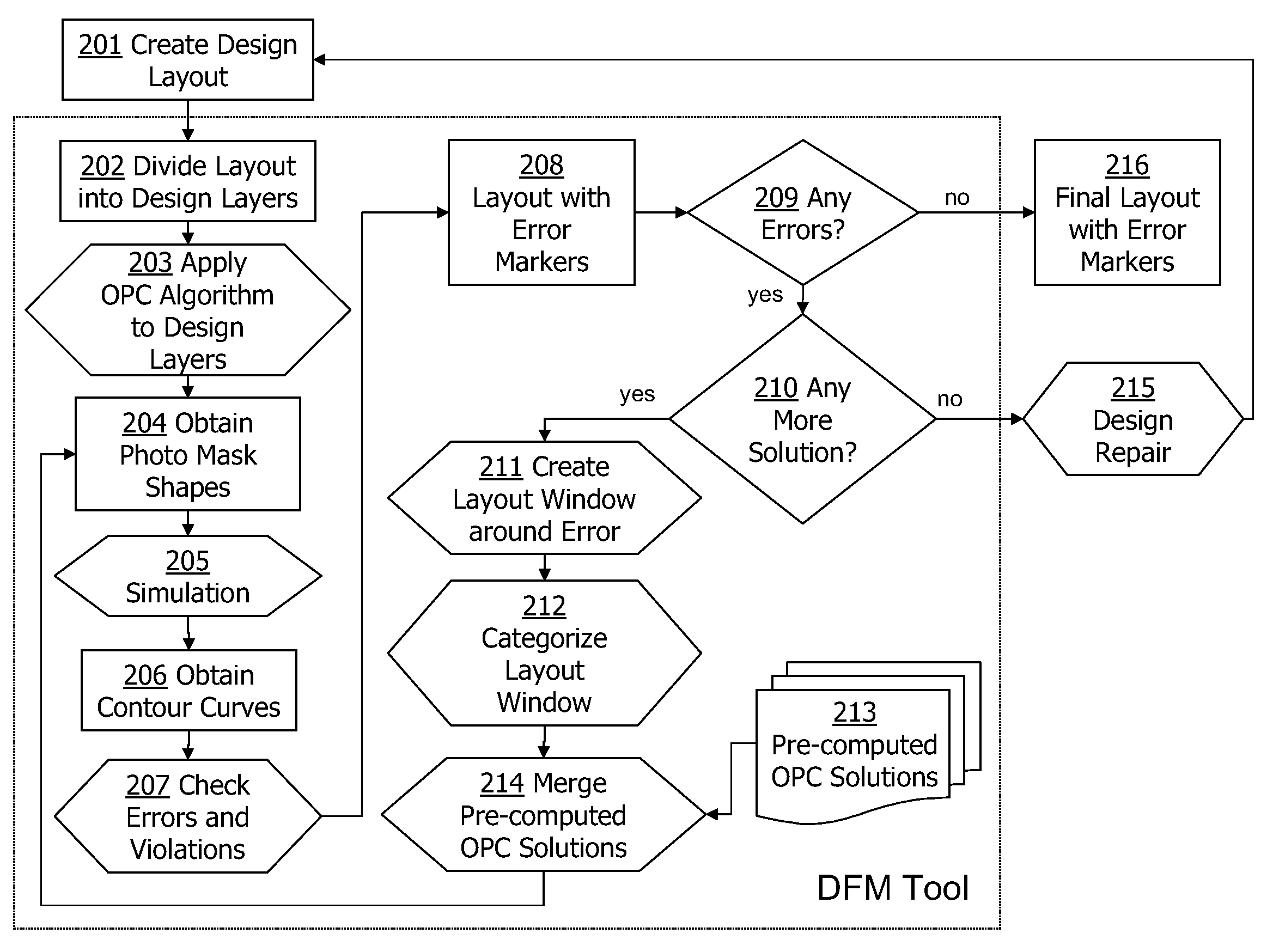
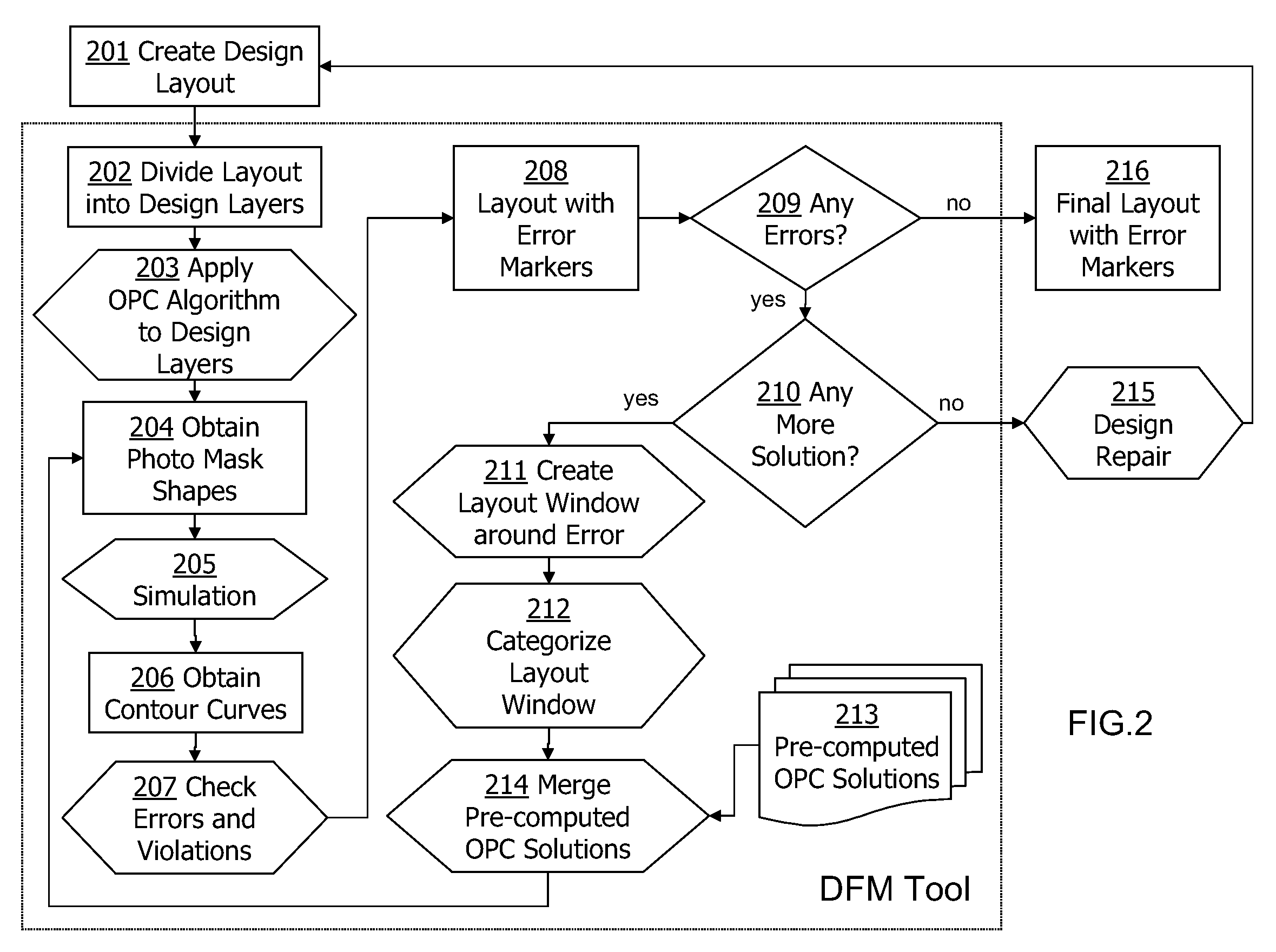
[0010]Embodiments of the present invention provide a method of performing photo-mask correction. The method includes steps of identifying a hot-spot in a photo-mask that violates one or more predefined rules; creating a window area in the photo-mask surrounding the hot spot; categorizing the window area; selecting a local solution from a library of pre-computed solutions based on the category of the window area; and applying the local solution to the hot spot.

[0011]In one embodiment, the step of categorizing the window area includes assigning a category to the window area based upon a type of violation of the hot spot being surrounded by the window area. In another embodiment, the pre-computed solutions are determined through improvement of both exposure source shapes and mask shapes.

[0012]In one embodiment, the method further include, if no solution is available from the library of pre-computed solutions based upon the category of the window area, repairing a design layout from whi...


PUM


Abstract

Embodiments of the present invention provide a method of performing photo-mask correction. The method includes identifying a hot-spot in a photo-mask that violates one or more predefined rules; creating a window area in the photo-mask that surrounds the hot spot; categorizing the window area; selecting a solution, from a library of pre-computed solutions, based on a category of the window area; and applying the solution to the hot spot. A service-oriented architecture (SOA) system that synchronizes the design to the process is also provided.

Description

FIELD OF THE INVENTION[0001]The present invention relates generally to optical lithography in the field of semiconductor device manufacturing and, more specifically, relates to method and system for making photo-mask corrections with enhanced resolution to improve quality of device pattern transferring.BACKGROUND OF THE INVENTION[0002]Today's semiconductor device manufacturing process has pushed resolution limits of certain tools and materials used in optical lithography to a point where catastrophic failures may occur for some configurations if not being designed carefully. In order to ensure that failing configurations do not occur in actual designs, manufacturers of semiconductor devices have typically relied upon some predefined design rules that device designers must follow. However, as geometries of device patterns continue to shrink, these design rules have often been found incapable of adequately safeguarding device patterns against all failure mechanisms.[0003]In order to p...

Claims


Application Information

Patent Timeline
IPC IPC(8): G06F17/50
CPCG03F1/36
Inventor GRAUR, IOANAMANSFIELD, SCOTT M.
Owner GLOBALFOUNDRIES INC
Why Eureka
Try Eureka