
Signal processing device

a signal processing and signal technology, applied in the field of signal processing devices, can solve the problems of distortion of low-frequency component of input data, inability to correct a/d conversion, loss of waveform proportion, etc., and achieve the effect of efficient offset control

Active Publication Date: 2010-07-29
PANASONIC SEMICON SOLUTIONS CO LTD
View PDF7 Cites 12 Cited by
  • Summary
  • Abstract
  • Description
  • Claims
  • Application Information

AI Technical Summary

Benefits of technology

[0055]According to the present invention, it is possible to provide a signal processing apparatus which can absorb a steep difference in DC component that is included in a reproduced signal, without increasing the number of terminals, by performing efficient offset control.

Problems solved by technology

As the DC offset increases, the reproduced signal waveform might exceed the input dynamic range of the A / D converter 3, which causes a problem that a portion of the waveform is lost and thereby correct A / D conversion cannot be performed.
On the other hand, when the time constant of the operation of the high-pass filter 8 is set short, there may occur a drawback that the low-frequency component of the input data has a distortion.
However, when using the resistor in the LSI, it is difficult to accurately produce a pair of resistors having a resistance value of about 10000 times. Further, since it is also difficult to produce a pair of capacitors having a capacitance value of 10000 times, it is necessary to adopt a configuration which enables switching of the capacitance value using a capacitor externally attached to the LSI as shown in FIG. 7, or a configuration which enables switching of the resistance value using an external resistor.

Method used


Image

  • Signal processing device
  • Signal processing device
  • Signal processing device

Examples


embodiment 1

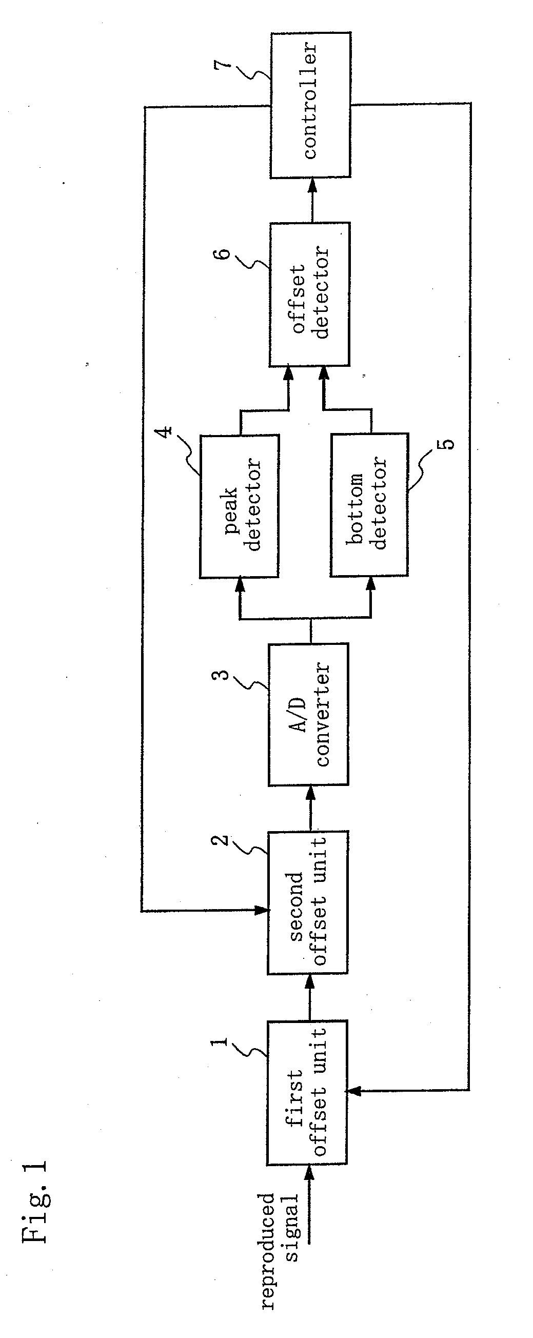
[0142]A first embodiment of the present invention corresponds to inventions disclosed in Claims 1 and 2, wherein first and second offset units are exclusively controlled based on offset information that is detected from sampling data outputted from an A / D converter 3, thereby enabling absorption of a DC offset component without increasing the number of terminals, and inputting of a signal so as to be within the input dynamic range of the A / D converter.

[0143]Hereinafter, the first embodiment of the present invention will be described in detail with reference to the drawings.

[0144]FIG. 1 is a block diagram of a signal processing device according to the first embodiment.

[0145]This signal processing device comprises a first offset unit 1 which gives a DC offset according to an offset control signal to an reproduced signal input, a second offset unit 2 which receives the output of the first offset unit 1 as an input signal and gives a DC offset according to an offset control signal to th...

embodiment 2

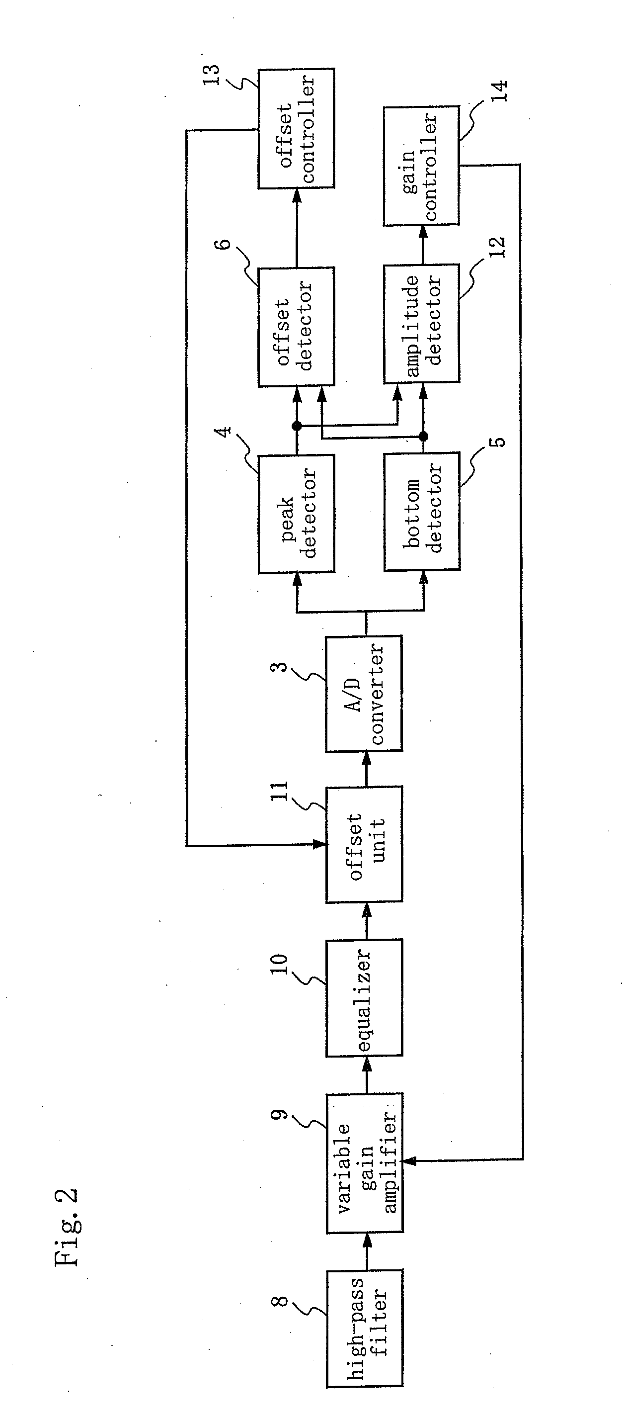
[0177]A second embodiment corresponds to the inventions disclosed in Claims 3, 4, 5, and 6, wherein the first and second offset units are exclusively controlled based on the offset information that is detected from the sampling data outputted from the A / D converter 3, thereby enabling absorption of a DC offset component without increasing the number of terminals, and inputting of the signal within the input dynamic range of the A / D converter.

[0178]Hereinafter, the second embodiment of the present invention will be described in detail with reference to the drawings. FIG. 19 is a block diagram of a signal processing device of this second embodiment.

[0179]The signal processing device comprises a first offset unit 1 which gives a DC offset according to an offset control signal to a reproduced signal input, a second offset unit 2 which receives an output of the first offset unit 1 as an input signal and gives a DC offset according to an offset control signal to the input signal, an A / D c...

embodiment 3

[0205]A third embodiment corresponds to the inventions of Claim 7 and Claim 8, wherein the first and second offset units are exclusively controlled based on the offset information that is detected from the sampling data outputted from the A / D converter 3, thereby enabling absorption of a DC offset component without increasing the number of terminals, and inputting of the signal within the input dynamic range of the A / D converter. Further, a storage unit is provided to hold a control value for the offset unit, thereby realizing efficient operation.

[0206]Hereinafter, the third embodiment of the present invention will be described in detail with reference to the drawings. FIG. 23 is a block diagram of a signal processing device of the third embodiment.

[0207]This signal processing device comprises a first offset unit 1 which gives a DC offset according to an offset control signal to a reproduced signal input, a second offset unit 2 which receives an output of the first offset unit 1 as ...


PUM


Abstract

It is an object of the present invention to provide a signal processing device which, even when a steep difference in DC level is included in a signal read from a disc such as a DVD-RAM format, cuts off the DC level and pulls the read signal into an appropriate A / D input level with an attempt to cost reduction. A steep difference in DC level between a data section and a CAPA section is absorbed by a first offset unit 1, and an asymmetry which occurs due to variations in the disc manufacturing stage is corrected by a second offset unit 2. Further, a control signal for operating the two offset units exclusively is generated by a controller 7, thereby to control the both offset units.

Description

TECHNICAL FIELD[0001]The present invention relates to a signal processing device which analog-to-digital converts data recorded on an information recording medium to reproduce the data. More particularly, the invention relates to an improvement of a technique for adjusting a DC voltage of an analog signal in order to efficiently use an input dynamic range of an A / D converter.BACKGROUND ART[0002]While an analog signal processing IC and a digital signal processing LSI have conventionally been configured in different chips, approaches for reducing circuit scale, footprint, and external parts by integrating these ICs in one chip have been made. Further, a cost-down effect due to semiconductor process shrinkage can be easily obtained by promoting digitization of analog signal processing circuits.[0003]With these approaches, the conventional signal processing circuit is required to perform efficient analog-to-digital conversion in a unit for converting an analog signal into a digital sign...

Claims


Application Information

Patent Timeline
IPC IPC(8): H03M1/12
CPCG11B20/10009G11B20/10027G11B20/10037G11B2220/2575G11B20/10203G11B2220/216G11B2220/2562G11B20/10046
Inventor KAIHARA, RIEOGURA, YOUICHI
Owner PANASONIC SEMICON SOLUTIONS CO LTD
Learn More