Semiconductor optical device

a technology of semiconductors and optical devices, applied in semiconductor lasers, optical elements, instruments, etc., can solve the problems of insufficient characteristics of semiconductor optical devices using semi-insulating substrates, and achieve the effect of removing the degradation of characteristics

Active Publication Date: 2010-07-29
LUMENTUM JAPAN INC
View PDF3 Cites 18 Cited by
  • Summary
  • Abstract
  • Description
  • Claims
  • Application Information

AI Technical Summary

Benefits of technology

[0009]Consequently, to eliminate the characteristics degradation due to the first cause, while maintaining the order of stacking the layers of a p-type semiconductor layer, an active layer and an n-type semiconductor layer from the substrate side as it is, the semi-insulating substrate itself is multilayered to be a multilayered semi-insulating substrate having a Ru—InP layer provided on a conductive InP substrate.
[0010]Further, to eliminate the characteristics degradation due to the second cause, the device structure is changed to have the order of stacking the layers as an n-type semiconductor layer, an active layer, and a p-type semiconductor layer from the substrate side, and a Ru—InP substrate is used as the semi-insulating substrate itself on which the multilayered body is stacked; and alternatively, the semi-insulating substrate itself is multilayered to be a multilayered semi-insulating substrate having a Ru—InP layer provided on an Fe—InP substrate. Note that, as same as the way to eliminate the characteristics degradation due to the first cause, the same effects can be achieved when a multilayered semi-insulating substrate having a Ru—InP substrate provided on a conductive InP substrate is used.
[0011]According to the present invention, characteristics of conventional semiconductor optical devices using a semi-insulating substrate can be improved.

Problems solved by technology

The semiconductor optical device using the semi-insulating substrate disclosed in Patent Document 1 described above cannot achieve sufficient characteristics.

Method used


Image

  • Semiconductor optical device
  • Semiconductor optical device
  • Semiconductor optical device

Examples


first embodiment

[0065

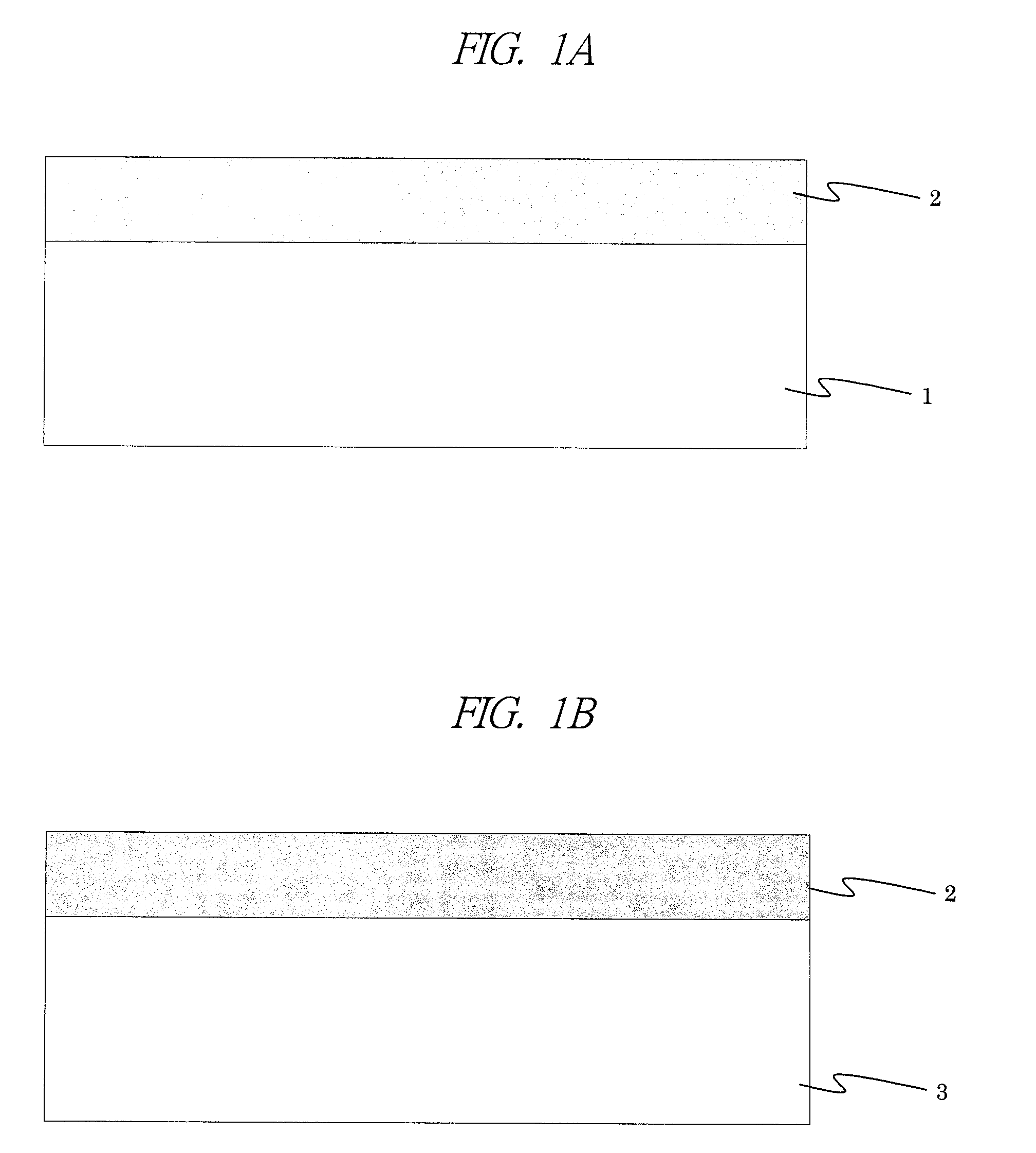
[0066]FIGS. 1A and 1B are cross-sectional views of an SI—InP substrate used in a first embodiment. FIG. 1A is a structure in which a Ru—InP layer is stacked on a Zn-doped InP substrate as a conductive InP substrate. FIG. 1B is a structure in which a Ru—InP layer is stacked on a S (sulfur)-doped InP substrate as a conductive InP substrate.

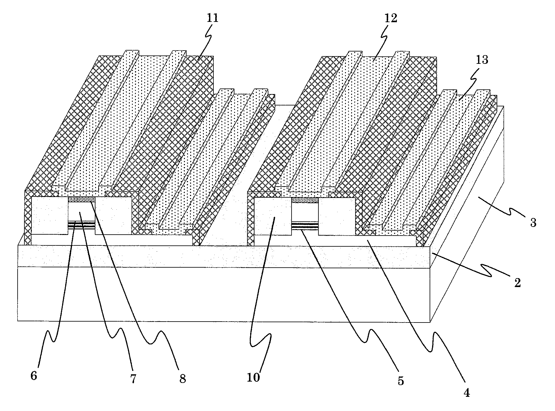
[0067]FIG. 3 is a perspective view of a semiconductor optical device according to the first embodiment, and FIG. 4 is a partial cross-sectional view of the semiconductor optical device described in FIG. 3 in an optical axis direction.

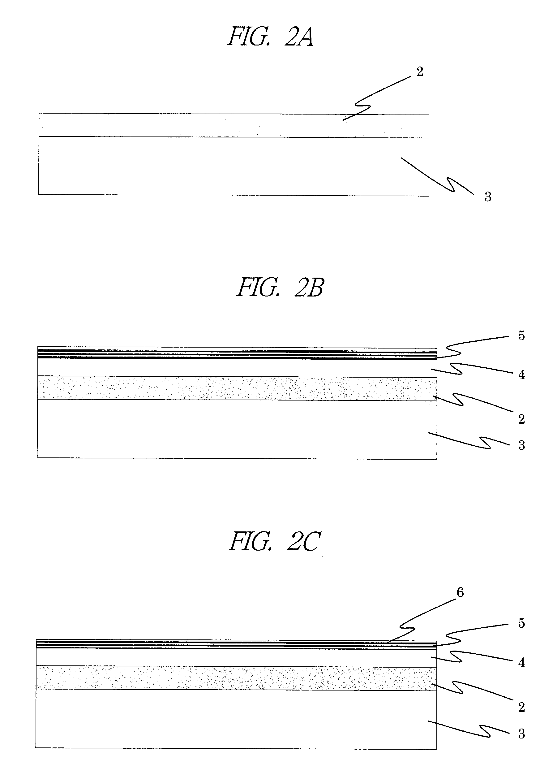
[0068]A manufacturing process of the semiconductor optical device according to the first embodiment using the SI—InP substrate in FIGS. 1A and 1B will be described with reference to FIGS. 2A to 2I. Note that the figure only describes the embodiment and the size of the figure is not necessarily the same with the scale and curvature mentioned in the present embodiment.

[0069]Here, while the descriptions will be made u...

second embodiment

[0077

[0078]FIG. 5 is a perspective view of a semiconductor optical device (optical electrical integrated device: OEIC) according to a second embodiment. The semiconductor optical device is an EA / DFB laser in which an EA modulator and a DFB laser are integrated. Note that the figure only describes the embodiment and the size of the figure is not necessarily the same with the scale and curvature mentioned in the present embodiment. Here, the descriptions will be made with reference to an n-InP substrate formed of S—InP, but a p-InP substrate formed of Zn—InP may be used. In addition, the description will be made about an example of using Ru—InP as the SI—InP layer on a conductive InP substrate, it can be Os—InP layer also

[0079]First, an SI—InP layer 2 to which Ru is doped is formed on an n-InP substrate 3 by MOCVD. Subsequently, an n-InP cladding layer 4 and an undoped quantum well structure are sequentially stacked. As the quantum well structure, a multiple-quantum-well 5 can be form...

third embodiment

[0086

[0087]FIG. 6 is a perspective view of a semiconductor optical device (optical electrical integrated device: OEIC) according to a third embodiment. The semiconductor optical device is a MZ / DFB laser. Note that the figure only describes the embodiment and the size of the figure is not necessarily the same with the scale and curvature mentioned in the present embodiment. Here, the descriptions will be made with reference to an n-InP substrate formed of S—InP, but a p-InP substrate formed of Zn—InP may be used. In addition, the description will be made about an example of using Ru—InP as the SI—InP layer on a conductive InP substrate, it can be an Os—InP layer also. Incidentally, as a method of forming the optical integrated device of the third embodiment can be easily suggested from the second embodiment, detailed descriptions will be omitted here.

[0088]By applying the present invention, characteristics of semiconductor integrated device arrays in which a Mach-Zehnder modulator an...


PUM


Abstract

A purpose is to provide a semiconductor optical device having good characteristics to be formed on a semi-insulating InP substrate. Firstly, a semi-insulating substrate including a Ru—InP layer on a conductive substrate is used. Secondly, a semi-insulating substrate including a Ru—InP layer on a Ru—InP substrate or an Fe—InP substrate is used and semiconductor layers of an n-type semiconductor layer, a quantum-well layer, and a p-type semiconductor layer are stacked in this order.

Description

CROSS-REFERENCE TO RELATED APPLICATION[0001]The present application claims priorities from Japanese Patent Application No. JP 2008-306963 filed on De. 2, 2008, and Japanese Patent Application No. JP 2009-263472 filed on Nov. 19, 2009, the contents of which are hereby incorporated by reference into this application.TECHNICAL FIELD OF THE INVENTION[0002]The present invention relates to a semiconductor optical device composed of a semiconductor layer formed on a semi-insulating substrate.BACKGROUND OF THE INVENTION[0003]Along with the rapid spread of broadband network, achieving high speed, down-sizing, and high function have been important issues regarding optical communication devices. On the background, there is an increasing need for a semiconductor optical device (OEIC device) including an optical electronic integrated circuit (OEIC) in which optical functional devices such as a semiconductor laser device, an optical modulator and a photodiode, which have been used as individual d...

Claims


Application Information

Patent Timeline
Patent Type & Authority Applications(United States)
IPC IPC(8): H01L29/20H01S5/125H01L31/107H01L31/105H01S5/12
CPCG02B6/12007H01S5/227G02B6/29344G02B6/29352G02B2006/12097G02B2006/121G02B2006/12159H01L21/02392H01L21/02461H01L21/02543H01L21/02581H01L31/03042H01L31/105H01L31/107H01S5/0208H01S5/0265H01S5/0425H01S5/12H01S5/125G02B6/12009H01S5/04257H01S5/04256
Inventor MAKINO, SHIGEKIKITATANI, TAKESHITSUCHIYA, TOMONOBU
Owner LUMENTUM JAPAN INC
Why Eureka
Try Eureka