Check patentability & draft patents in minutes with Patsnap Eureka AI!

Image sensor of stacked layer structure and manufacturing method thereof

a technology of image sensor and layer structure, applied in the direction of electrical equipment, semiconductor devices, radio frequency control devices, etc., can solve the problems of high production cost, complicated production process, and limited use of methods,

Inactive Publication Date: 2010-08-05
SILICONFILE TECH INC
View PDF3 Cites 16 Cited by
  • Summary
  • Abstract
  • Description
  • Claims
  • Application Information

AI Technical Summary

Benefits of technology

[0011]The present invention also provides a method of manufacturing a stacked image sensor by using a simple process for depositing a photosensitive element portion having a photo-conductive thin film on a wafer where a circuit is formed.

Problems solved by technology

However, the above method of manufacturing the stacked image sensor has complicated production processes and high production cost.
In addition, since alignment of two wafers needs to be performed at a high accuracy, the method has been used for a limited purpose.
Since electrodes, gates of transistors, and metal layers on the wafer are formed through impurity doping, there is a problem in that high-temperature processes such as a crystal growing process cannot be used.

Method used


Image

  • Image sensor of stacked layer structure and manufacturing method thereof
  • Image sensor of stacked layer structure and manufacturing method thereof
  • Image sensor of stacked layer structure and manufacturing method thereof

Examples


Embodiment Construction

[0021]Hereinafter, embodiments of the present invention will be described in detail with reference to the accompanying drawings.

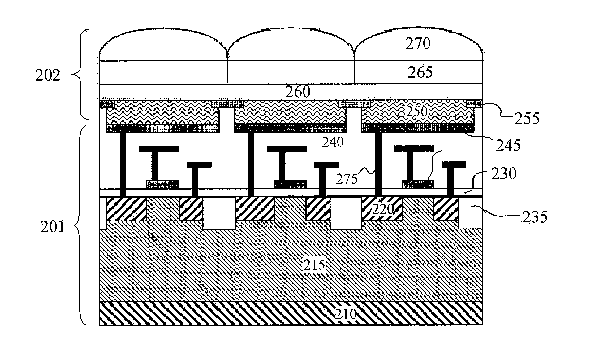
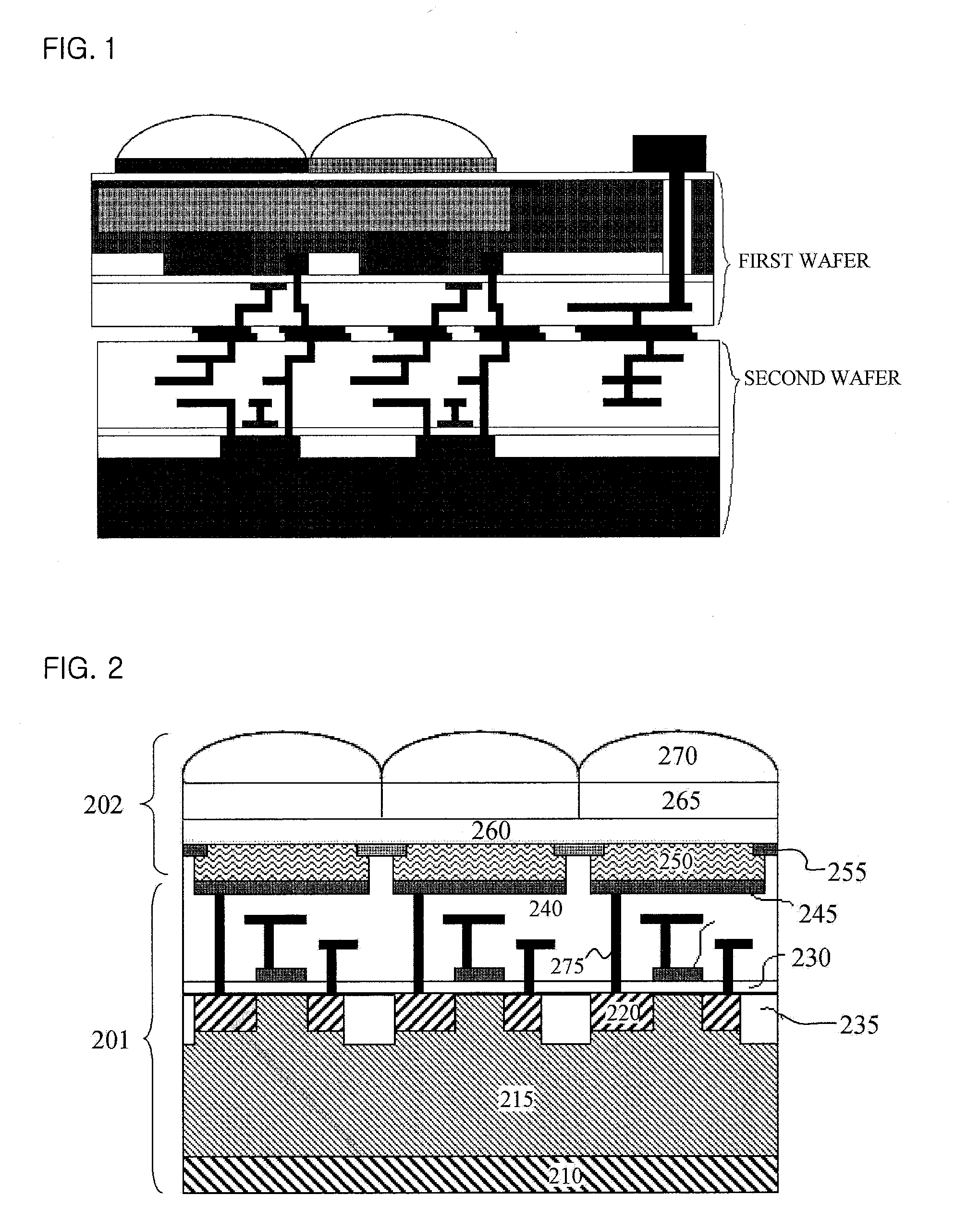
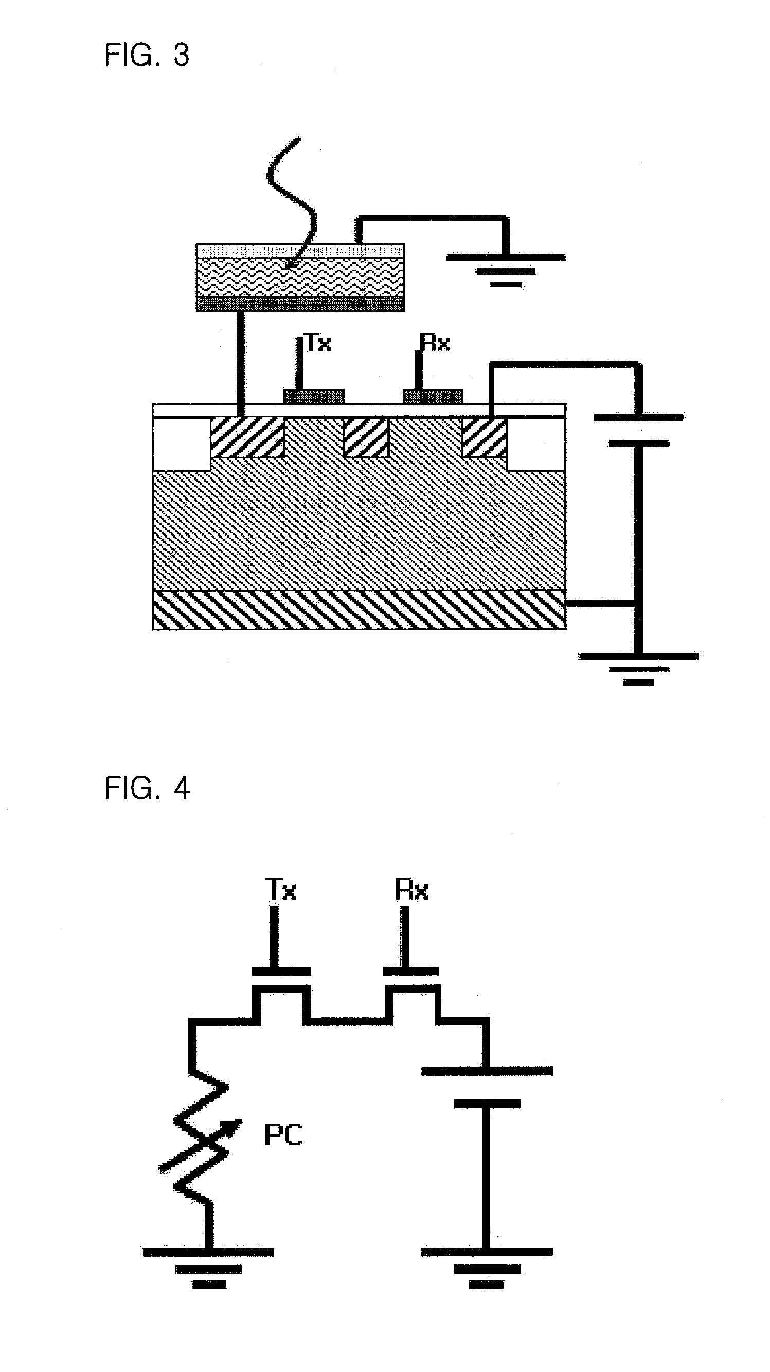
[0022]FIG. 2 is a schematic view illustrating a structure of a stacked image sensor according to the present invention.

[0023]Referring to FIG. 2, the stacked image sensor according to the present invention includes a wafer 201 where peripheral circuits are formed and a photosensitive element portion 202 formed on an upper portion of the wafer, and the photosensitive element portion 202 has a photo-conductive thin film 250.

[0024]The wafer 201 includes a first conductive type high-concentration doped semiconductor substrate 210, a first conductive type low-concentration epitaxial layer 215 formed on the semiconductor substrate, a gate oxide layer 230 formed on the epitaxial layer, one or more transistor gates 225 formed on the gate oxide layer 230, a second conductive type electrode 220 formed on an upper portion of the epitaxial layer, a trench 235 for isola...


PUM


Abstract

Provided is a stacked image sensor. Particularly, provided are a stacked image sensor including a photosensitive element portion having a photo-conductive thin film on an upper portion of a wafer where a peripheral circuit is formed and a method of manufacturing the stacked image sensor. In the stacked image sensor according to the present invention, since a wafer where a circuit is formed and a photosensitive element portion are formed in a stacked structure, a whole size of the image sensor can be reduced, and there is no optical crosstalk due to absorption of incident light to adjacent pixels. In addition, since a photo-conductive element having a high light absorbance is used, a high photo-electric conversion efficiency can be obtained. In addition, in the method of manufacturing a stacked image sensor according to the present invention, since the upper photosensitive element can be formed by using a simple low-temperature process, a production cost can be reduced.

Description

BACKGROUND OF THE INVENTION[0001]1. Field of the Invention[0002]The present invention relates to a stacked image sensor, and more particularly, to a stacked image sensor including a photosensitive element portion having a photo-conductive thin film on an upper portion of a wafer where a peripheral circuit is formed and a method of manufacturing the stacked image sensor.[0003]2. Description of the Related Art[0004]A stacked image sensor is a sensor where a photo-sensitive element such as a photodiode and peripheral circuits such as MOS (Metal Oxide Semiconductor) transistors are formed in a stacked structure.[0005]Since the photosensitive element such as a photodiode is disposed in an upper portion of the image sensor, a path of incident light in the stacked image sensor becomes short. Therefore, there is no optical crosstalk due to interference between adjacent pixels. Since a photodiode region and a MOS transistor region are disposed in the stacked structure, a size of the image se...

Claims


Application Information

Patent Timeline
IPC IPC(8): H01L31/0232H01L31/113
CPCH01L27/14667H01L27/14627H01L27/14H01L27/146
Inventor LEE, BYOUNG-SU
Owner SILICONFILE TECH INC
Features
  • R&D
  • Intellectual Property
  • Life Sciences
  • Materials
  • Tech Scout
  • Unparalleled Data Quality
  • Higher Quality Content
  • 60% Fewer Hallucinations
Learn More