Plastic capacitive touch screen and method of manufacturing same
- Summary
- Abstract
- Description
- Claims
- Application Information
AI Technical Summary
Benefits of technology
Problems solved by technology
Method used
Image
Examples
Embodiment Construction
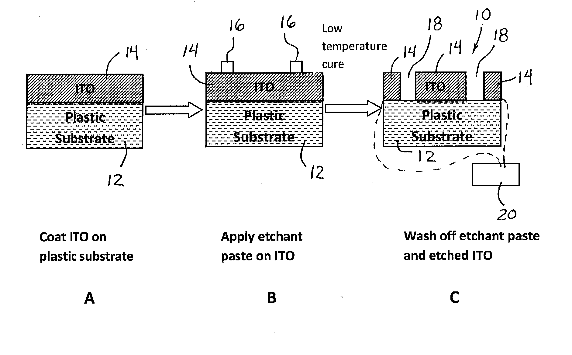
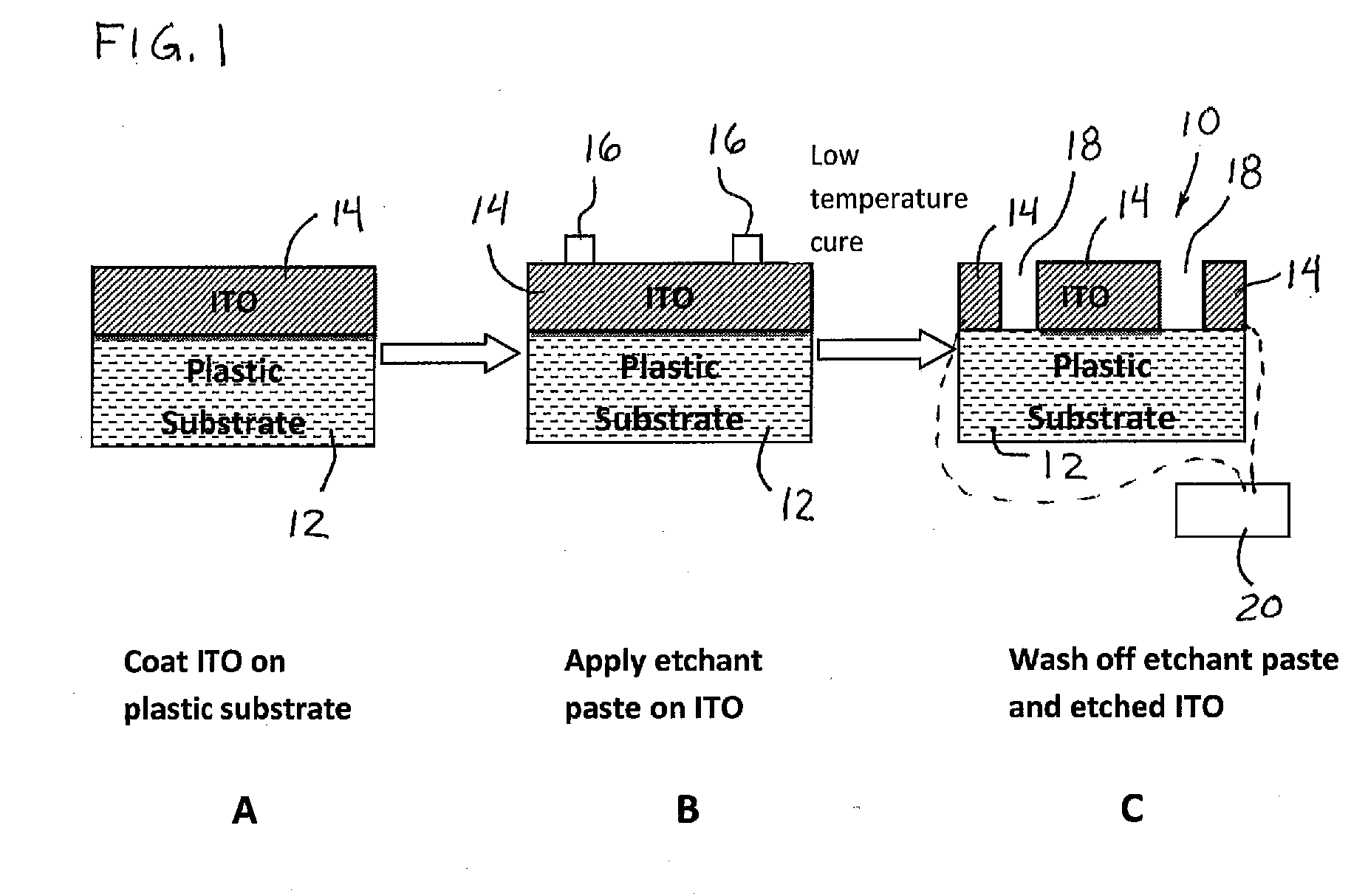
[0011]Referring now to the drawings and the illustrative embodiments depicted therein, a touch sensor 10 manufactured in accordance with the present invention as shown in FIG. 1. In the illustrated embodiment, the touch sensor includes a rigid or flexible substrate 12 (such as a plastic or polymeric substrate or the like) with a conductive layer 14 (such as a transparent conductive coating or layer comprising a transparent conductive material such as a transparent conductive overcoat (TCO) or indium tin oxide (ITO) or the like) disposed on a surface thereof (see A in FIG. 1). A pattern 18 is established in or at or through the transparent conductive layer via a removal process to electrically isolate portions of the conductive layer on the plastic substrate. For example, and as shown in FIG. 1, an etchant paste 16 is disposed on the conductive layer in a pattern (see B in FIG. 1), and the etchant paste is washed off the substrate after the paste has etched the pattern 18 into the co...
PUM
| Property | Measurement | Unit |
|---|---|---|
| Thickness | aaaaa | aaaaa |
| Temperature | aaaaa | aaaaa |
| Electrical conductor | aaaaa | aaaaa |
Abstract
Description
Claims
Application Information
 - R&D
- Intellectual Property
- Life Sciences
- Materials
- Tech Scout
- Unparalleled Data Quality
- Higher Quality Content
- 60% Fewer Hallucinations
Browse by: Latest US Patents, China's latest patents, Technical Efficacy Thesaurus, Application Domain, Technology Topic, Popular Technical Reports.
© 2025 PatSnap. All rights reserved.Legal|Privacy policy|Modern Slavery Act Transparency Statement|Sitemap|About US| Contact US: help@patsnap.com


