

Method for Fabricating a Semiconductor Component Based on GaN
a technology of semiconductor components and gan, applied in the direction of semiconductor/solid-state device manufacturing, semiconductor devices, electrical equipment, etc., can solve the problems of negligible and general minor deviations, and achieve the effect of increasing radiation output and simple technology
- Summary
- Abstract
- Description
- Claims
- Application Information
AI Technical Summary
Benefits of technology
Problems solved by technology
Method used
Image

Examples
Embodiment Construction
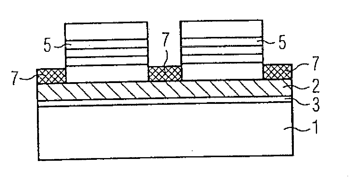
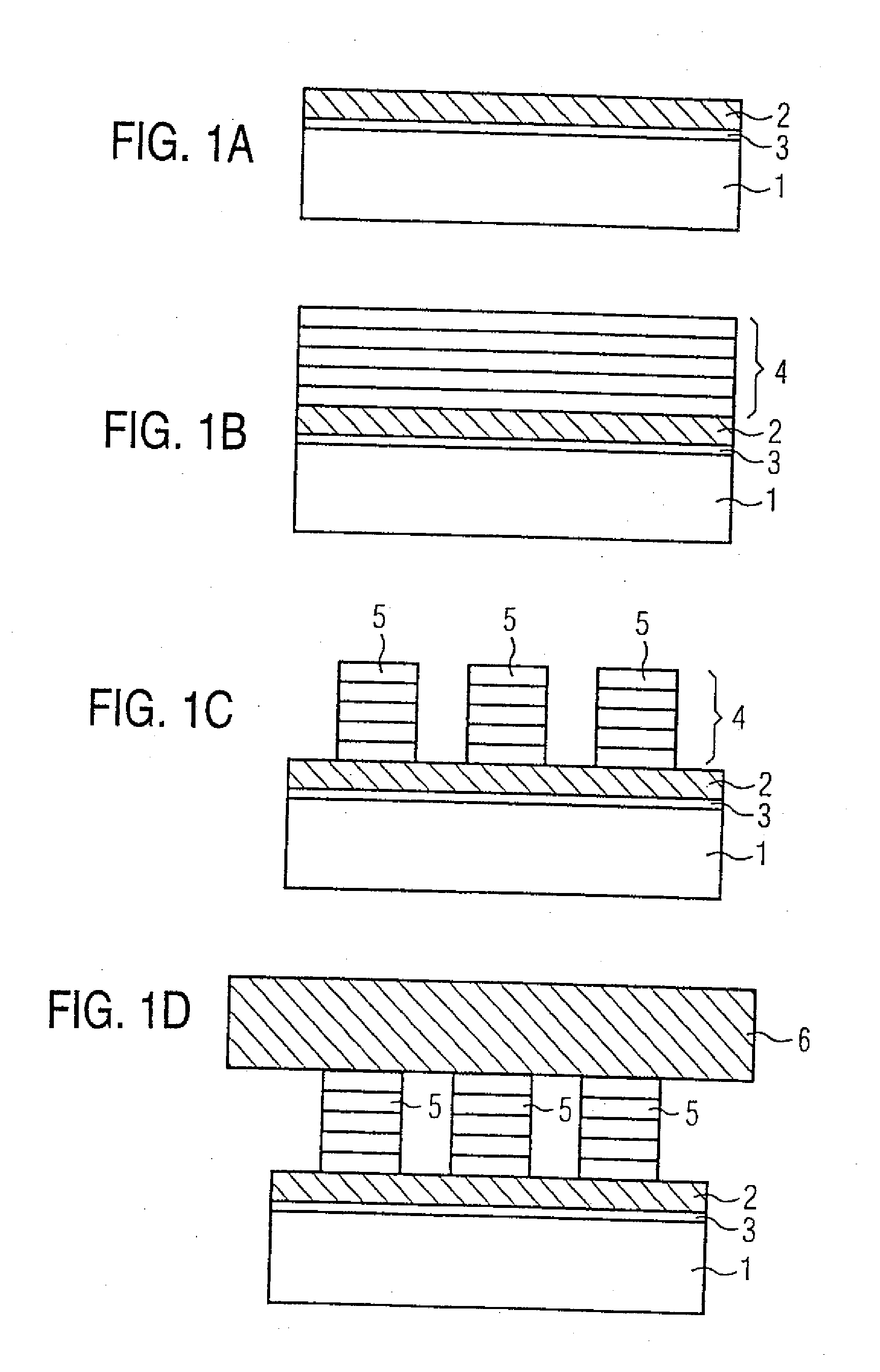
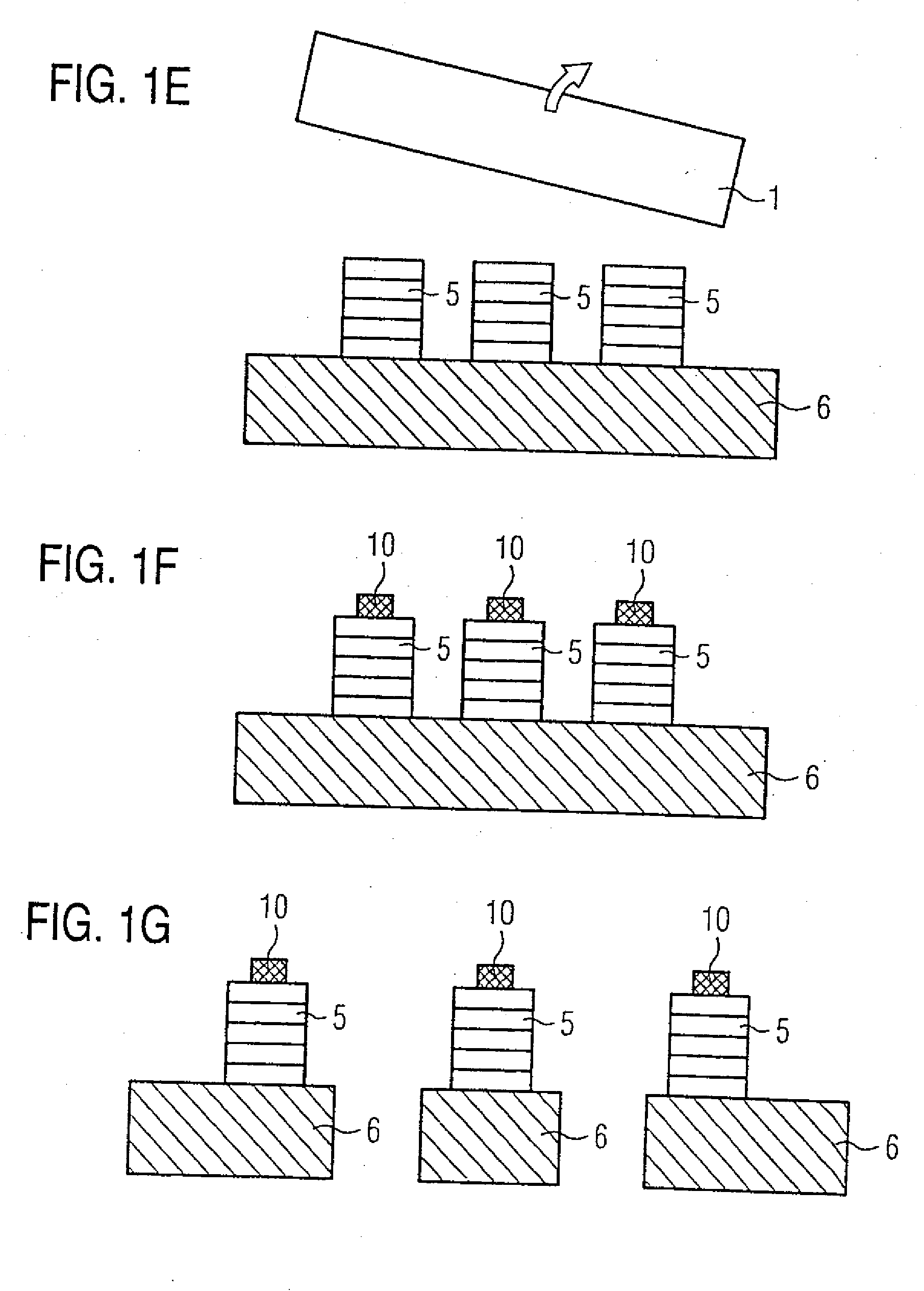
[0043]In all the figures of the drawing, sub-features and integral parts that correspond to one another bear the same reference symbol in each case. Referring now to the figures of the drawing in detail and first, particularly, to FIGS. 1A-1G thereof, there is shown a fabrication method. A composite substrate has a substrate body 1 made from poly-SiC to which a monocrystalline SiC interlayer 2 has been bonded in a known way is used. For this bonding, a bonding layer 3, for example of silicon oxide, has been formed between the substrate body 1 and the interlayer 2, see FIG. 1A.
[0044]A plurality of GaN-based layers 4 are grown epitaxially onto the composite substrate, FIG. 1B. The structure of the layer sequence is not in principle subject to any particular restrictions.
[0045]In this case, it is preferable to form an active layer that is used to generate radiation and is surrounded by one or more cladding layers and / or waveguide layers. The active layer may in this case be formed by a...
PUM
| Property | Measurement | Unit |
|---|---|---|
| semiconductor | aaaaa | aaaaa |
| electrically conductive | aaaaa | aaaaa |
| coefficient of thermal expansion | aaaaa | aaaaa |
Abstract
Description
Claims
Application Information