Manufacturing method for a semiconductor device
- Summary
- Abstract
- Description
- Claims
- Application Information
AI Technical Summary
Benefits of technology
Problems solved by technology
Method used
Image

Examples
first embodiment
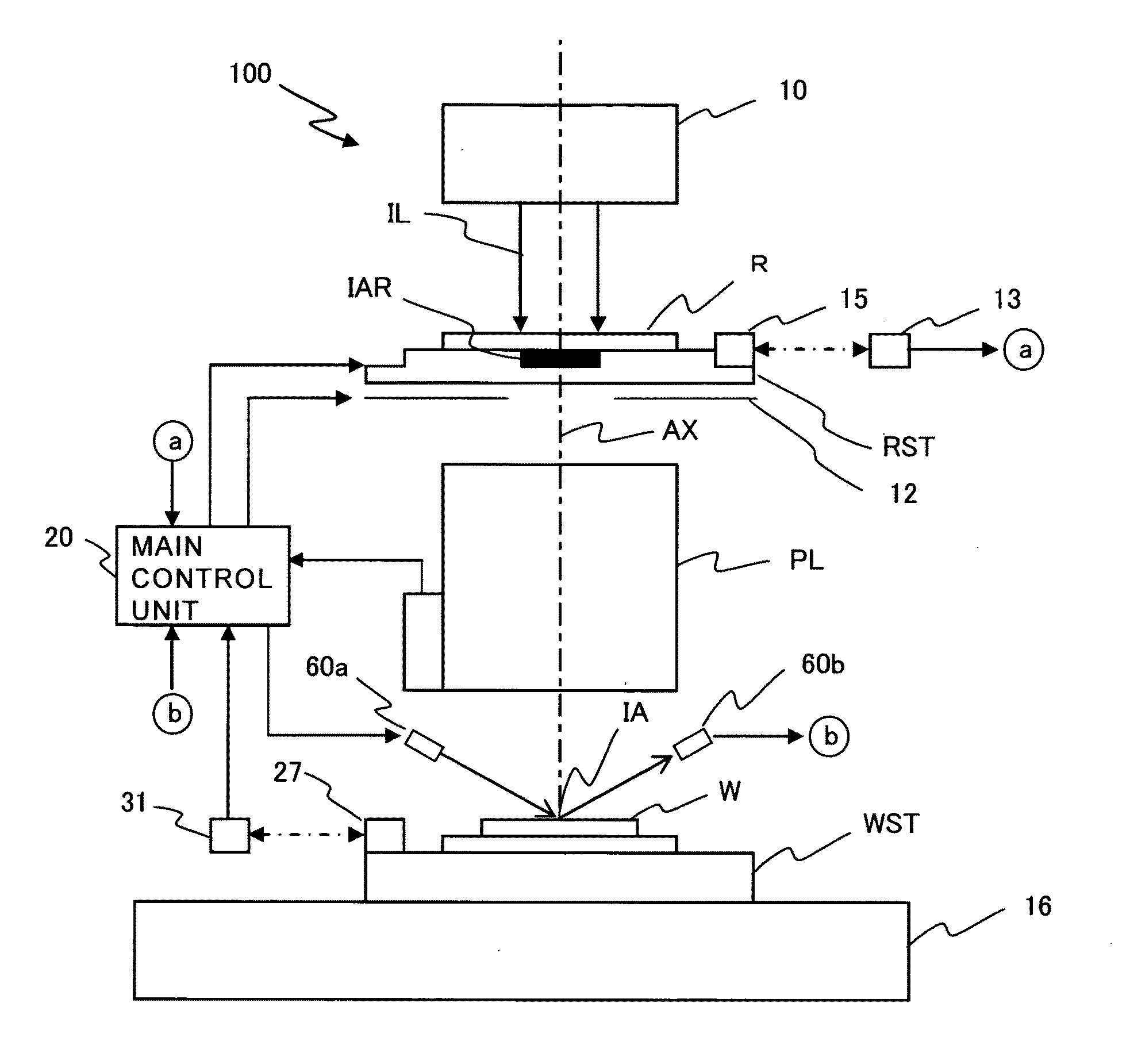
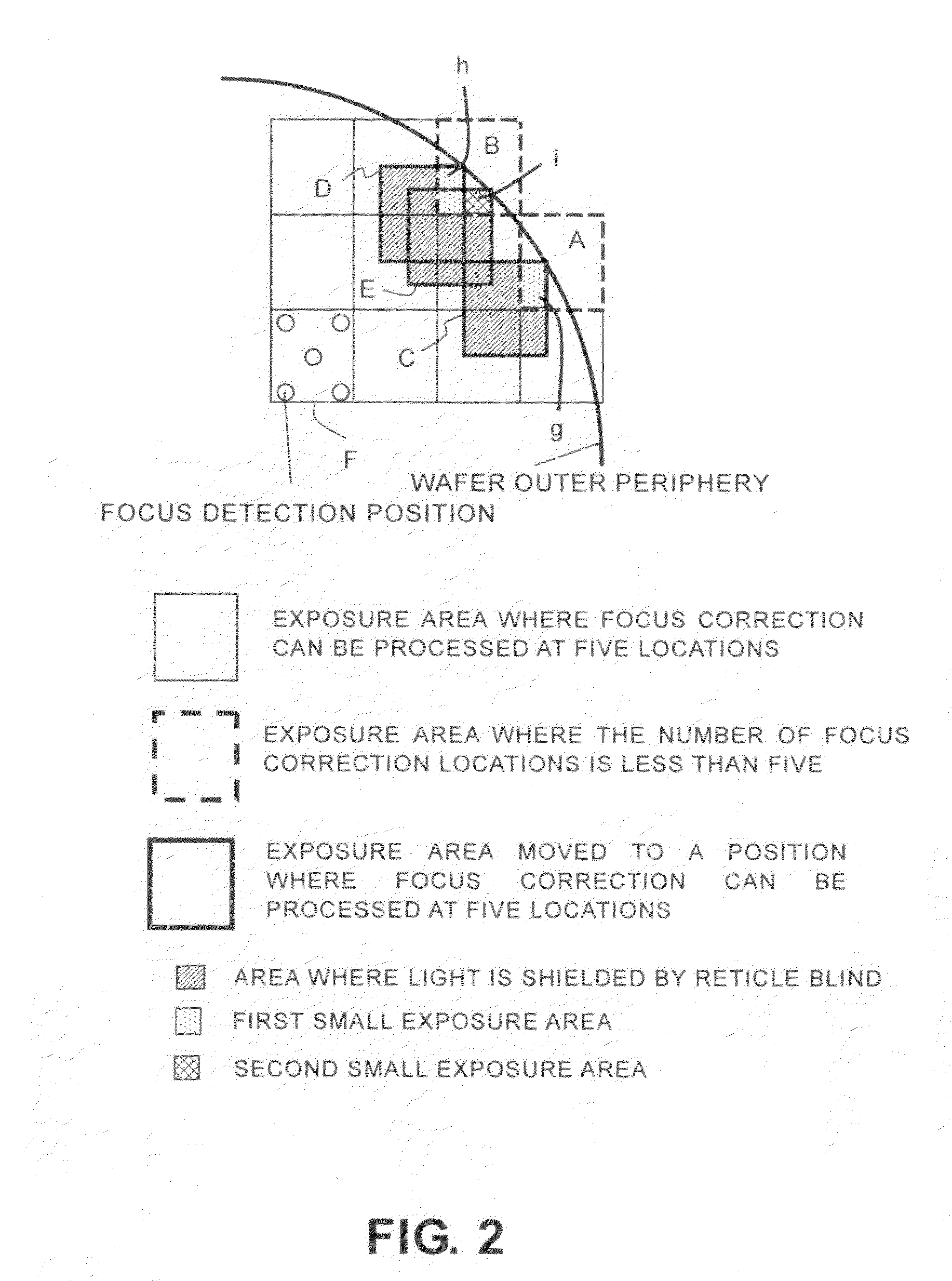
[0041]Then, the present invention is described with reference to FIG. 2.
[0042]FIG. 2 illustrates an exposure area (shot) at the wafer outer periphery according to the embodiment of the present invention.
[0043]One exposure area of the exposure device 100 is about 20 mm×20 mm, and therefore an exposure process for a sheet of wafer is completed through exposure of several ten times. Among a plurality of exposure areas, an exposure area being a start point is selected to a position where focus correction is enabled at five positions within a shot. In a shot F illustrated in FIG. 2, the focus detection positions at five positions are included within the shot, the focus correction processing is enabled, and an appropriate pattern may be formed over the entire shot. The exposure area such as the shot F is set as the start point, and the exposure processing is then performed on an adjacent exposure area.
[0044]When the exposure area comes to the wafer outer periphery, there is a case, howeve...
second embodiment
[0046]Subsequently, a second embodiment is described with reference to a shot B in FIG. 2.
[0047]In the shot B, similarly to the shot A, the focus detection cannot be performed at four positions within the shot, and the entire shot B cannot be appropriately autofocused or autoleveled. Under the above circumstance, the subsequent exposure area is not moved to the shot B, but moved to a position of a shot D where the entire shot is included in the wafer surface. At the position of the shot D, the focus detection is performed at five positions, and on the basis of the detection information, the shot D is autofocused or autoleveled. The adjacent exposure area is, then, shielded from light by the reticle blind to expose only a first small exposure area h. With the above operation, double exposure of the adjacent exposure area may be avoided. The subsequent exposure area is, then, moved to a position of a shot E where the entire shot is included in the wafer surface.
[0048]At the position o...
PUM
 Abstract
Description
Claims
Application Information
 - Generate Ideas
- Intellectual Property
- Life Sciences
- Materials
- Tech Scout
- Unparalleled Data Quality
- Higher Quality Content
- 60% Fewer Hallucinations
Browse by: Latest US Patents, China's latest patents, Technical Efficacy Thesaurus, Application Domain, Technology Topic, Popular Technical Reports.
© 2025 PatSnap. All rights reserved.Legal|Privacy policy|Modern Slavery Act Transparency Statement|Sitemap|About US| Contact US: help@patsnap.com