Semiconductor device fabrication method

Inactive Publication Date: 2010-08-12
CANON KK
View PDF21 Cites 22 Cited by
  • Summary
  • Abstract
  • Description
  • Claims
  • Application Information

AI Technical Summary

Benefits of technology

[0007]The present invention provides a highly inte

Problems solved by technology

It is difficult to obtain a highly integrated, low-noise, high-speed semic

Method used


Image

  • Semiconductor device fabrication method
  • Semiconductor device fabrication method
  • Semiconductor device fabrication method

Examples


Example

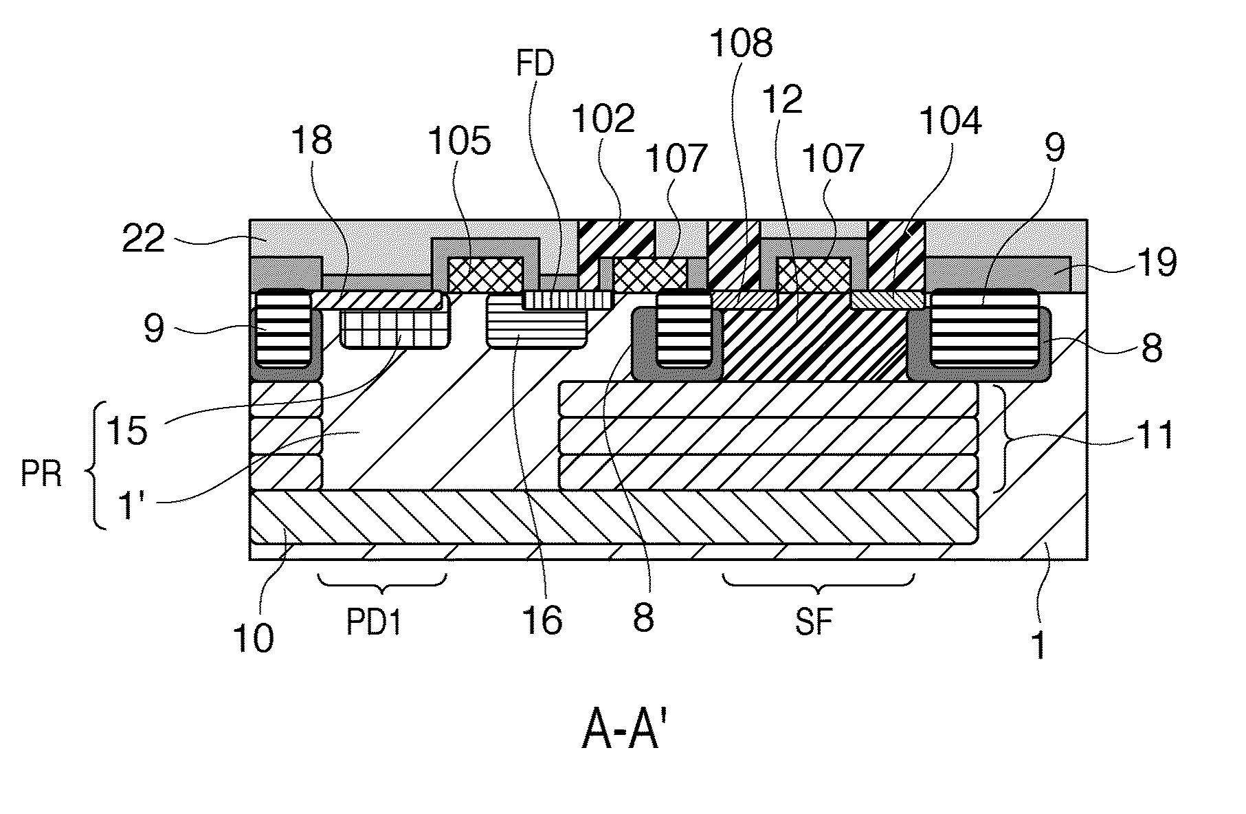
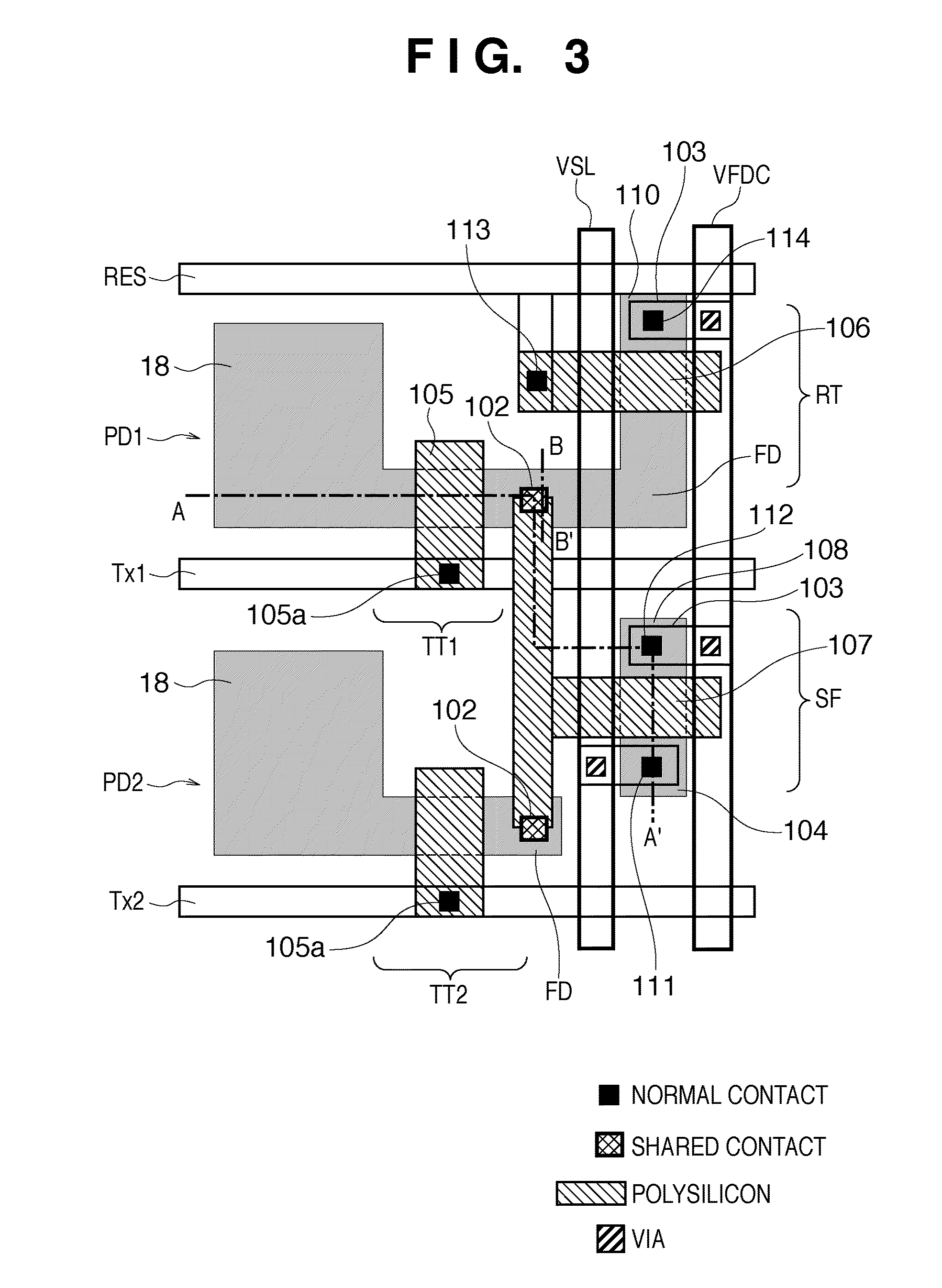
[0023]Embodiments of the present invention will be explained below with reference to the accompanying drawing.

[0024]The present invention is applicable to the fabrication of every semiconductor device having a shared contact plug that connects two regions different in conductivity type, for example, the fabrication of a photoelectric conversion device. In the following description, an example in which the present invention is provided to the fabrication of a photoelectric conversion device will be explained in order to provide a more practical example. However, the present invention can also be applied to the fabrication of other semiconductor devices such as a memory circuit, analog circuit, and logic circuit.

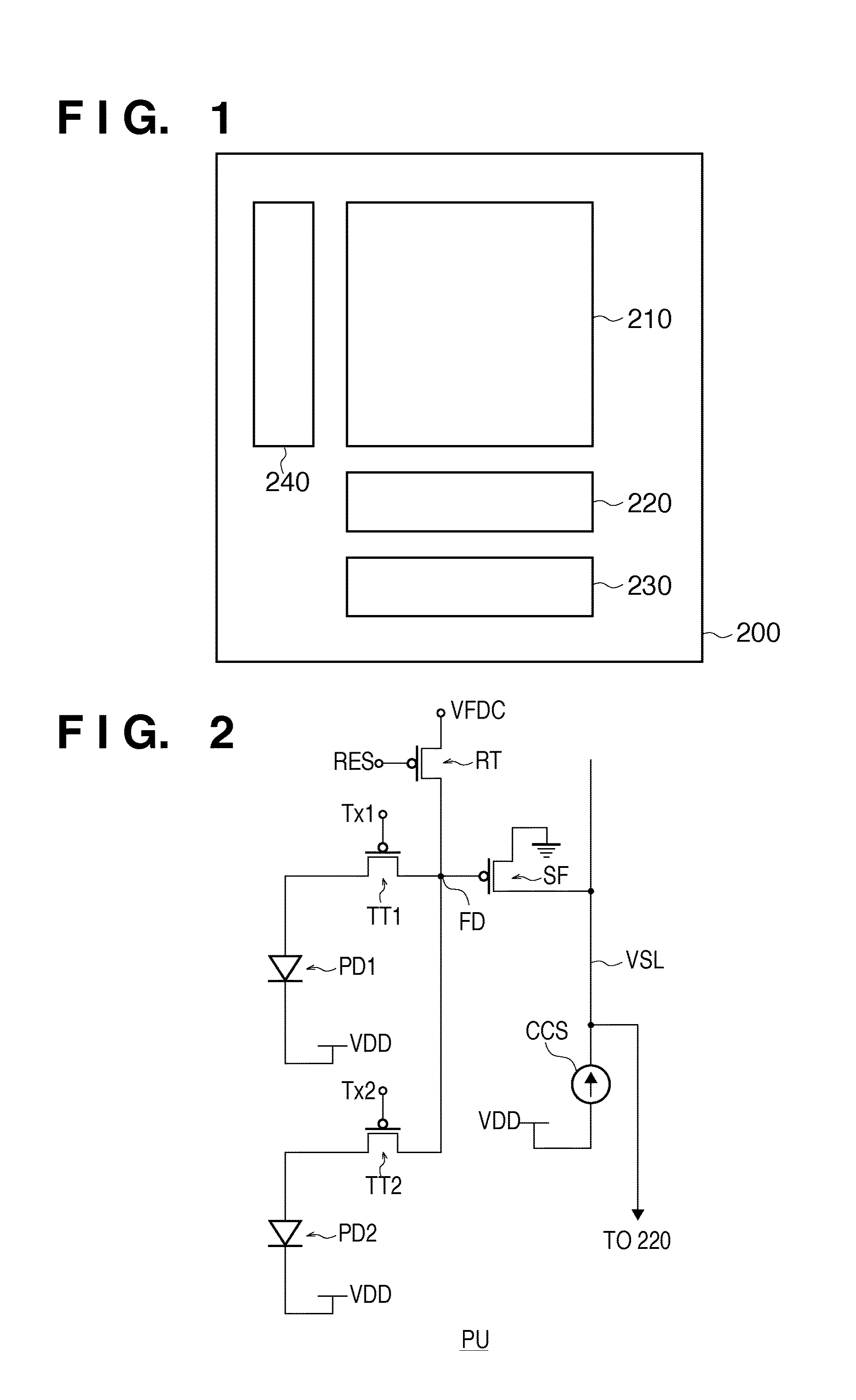
[0025]FIG. 1 is a view showing an outline of the arrangement of an image sensing device 200 of an embodiment of the present invention. The image sensing device 200 is formed on a semiconductor substrate, and can be called a solid-state image sensor, MOS image sensor, CMOS sens...


PUM


Abstract

A method of fabricating a semiconductor device, comprises steps of forming a common contact hole for a first conductivity-type region and a second conductivity-type region, implanting an impurity in at least one of the first conductivity-type region and the second conductivity-type region, and forming a shared contact plug by filling an electrical conducting material in the contact hole, wherein in the implanting step, an impurity is implanted in at least one of the first conductivity-type region and the second conductivity-type region such that the first conductivity-type region and the shared contact plug are brought into ohmic contact with each other, and the second conductivity-type region and the shared contact plug are brought into ohmic contact with each other.

Description

BACKGROUND OF THE INVENTION[0001]1. Field of the Invention[0002]The present invention relates to a semiconductor device fabrication method.[0003]2. Description of the Related Art[0004]Japanese Patent Laid-Open No. 2008-85304 relates to a method of fabricating a MOS photoelectric conversion device. This reference has disclosed a technique by which the gate of an amplifier MOS transistor in a pixel is connected to a floating diffusion by a shared contact plug. The shared contact technique is advantageous in downsizing semiconductor devices.[0005]Japanese Patent Laid-Open No. 2008-85304 does not mention the relationship between the conductivity type or impurity concentration of a diffusion region to be connected by the shared contact plug and the conductivity type or impurity concentration of the gate of a MOS transistor.[0006]When two regions to be connected by the shared contact plug have opposite conductivity types, the shared contact plug must be brought into ohmic contact with bot...

Claims


Application Information

Patent Timeline
IPC IPC(8): H01L21/768
CPCH01L21/76895H01L27/14689H01L27/14643
Inventor OHTANI, AKIRAWATANABE, TAKANORIICHIKAWA, TAKESHI
Owner CANON KK
Why Eureka
Try Eureka