Epitaxial Lift Off in Inverted Metamorphic Multijunction Solar Cells

a solar cell, inverted metamorphic technology, applied in the field of semiconductor devices, can solve the problems of presenting a number of practical difficulties, unable to produce a commercially viable and energy efficient inverted metamorphic multijunction solar cell using commercially established fabrication processes, and a more complex manufacturing process, etc., to achieve similar indices of refraction

Inactive Publication Date: 2010-08-12
EMCORE SOLAR POWER
View PDF99 Cites 73 Cited by
  • Summary
  • Abstract
  • Description
  • Claims
  • Application Information

AI Technical Summary

Benefits of technology

[0031]In another aspect the present invention provides a method of manufacturing a solar cell comprising providing a first substrate; depositing a separation layer on the first substrate; depositing a sequence of layers of semiconductor material forming a solar cell including at least one pair of adjacent layers have different composition and substantially similar indices of ...

Problems solved by technology

Compared to silicon, III-V compound semiconductor multijunction devices have greater energy conversion efficiencies and generally more radiation resistance, although they tend to be more complex to manufacture.
However, the materials and structures for a number of different layers of the cell proposed and described in such reference present a number of practical difficulties, particularly ...

Method used


Image

  • Epitaxial Lift Off in Inverted Metamorphic Multijunction Solar Cells
  • Epitaxial Lift Off in Inverted Metamorphic Multijunction Solar Cells
  • Epitaxial Lift Off in Inverted Metamorphic Multijunction Solar Cells

Examples


second embodiment

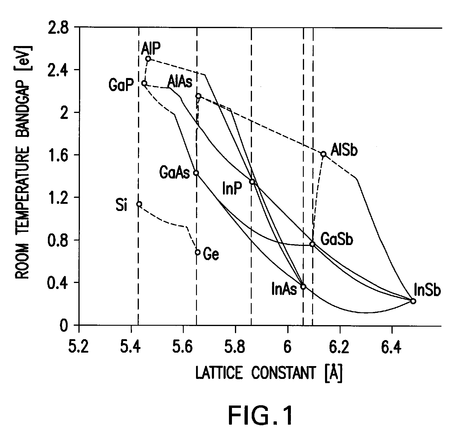
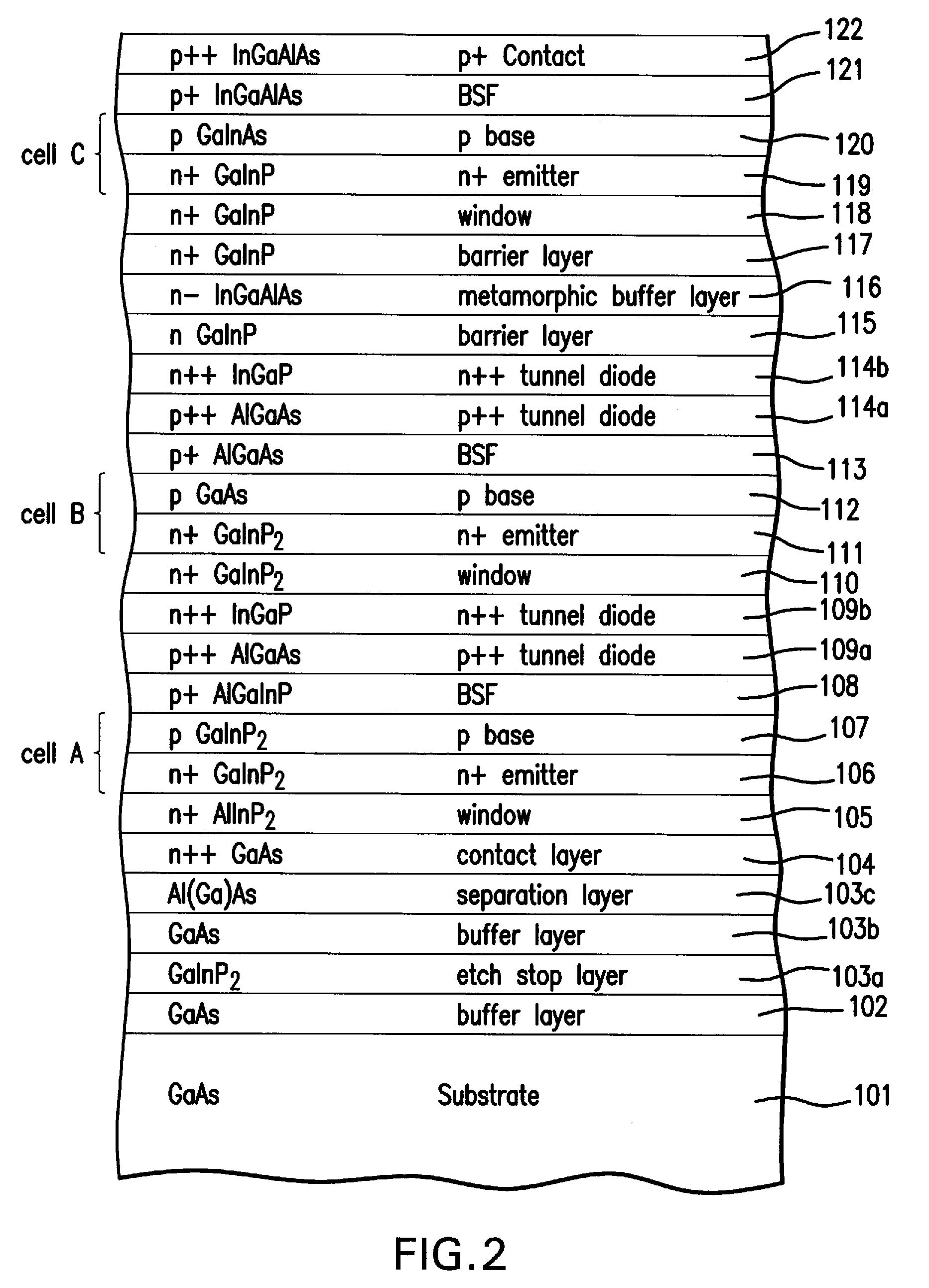
[0096]Although the preferred embodiment of the present invention utilizes a plurality of layers of InGaAlAs for the metamorphic layer 116 for reasons of manufacturability and radiation transparency, other embodiments of the present invention may utilize different material systems to achieve a change in lattice constant from subcell B to subcell C. Thus, the system of Wanlass using compositionally graded InGaP is the present invention. Other embodiments of the present invention may utilize continuously graded, as opposed to step graded, materials. More generally, the graded interlayer may be composed of any of the As, P, N, Sb based III-V compound semiconductors subject to the constraints of having the in-plane lattice parameter greater or equal to that of the second solar cell and less than or equal to that of the third solar cell, and having a bandgap energy greater than that of the second solar cell.

[0097]In another embodiment of the present invention, an optional second barrier l...

first embodiment

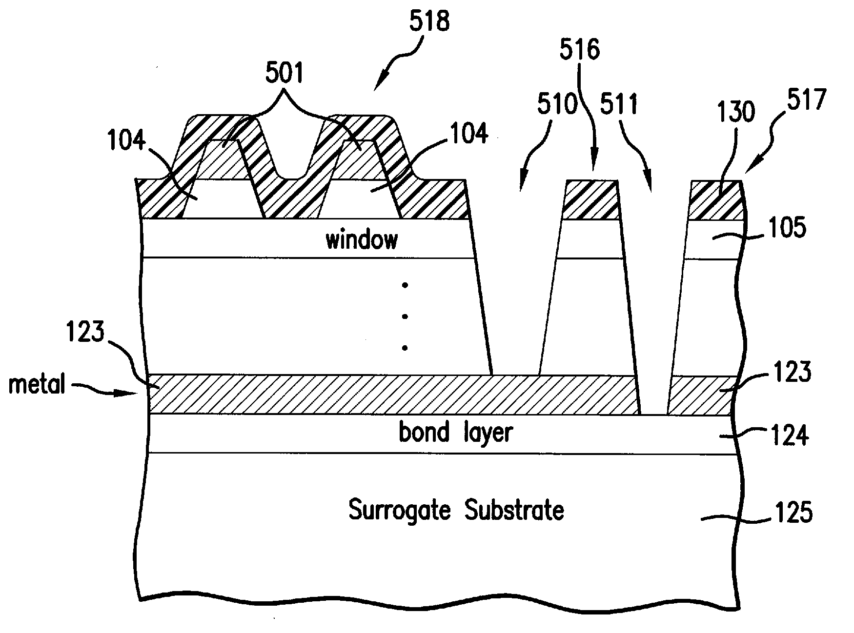
[0111]FIG. 8A is a side elevational view showing an epitaxially grown thin film semiconductor device being peeled from an underlying single crystal substrate by the etching technique generally according to the present invention. The semiconductor structure is immersed in a container 207 holding the etchant solution 206, and the figure depicts the surrogate substrate 125 and the epitaxial layers being released from the substrate 100, as the bubbles or reaction products 208 are released from the region of the separation layer 103c. The specific mechanical lifting technique depicted in FIG. 7 is only one representative embodiment, and accordingly the link elements 204 attached to a pulley 205 are not depicted to simplify the drawing.

[0112]FIG. 8B is a side elevational view showing an epitaxially grown thin film semiconductor device being peeled from an underlying single crystal substrate by the etching technique according to a second embodiment of the present invention. The semiconduct...

third embodiment

[0113]FIG. 8C is a side elevational view showing an epitaxially grown thin film semiconductor device being peeled from an underlying single crystal substrate by the etching technique according to the present invention. The semiconductor structure is immersed in a container 207 holding the etchant solution 206. A pliable member 211 is attached to the back surface of the surrogate substrate 125. A funnel shaped member 212 is attached to the center of the pliable member 211. Air suction 213 is then applied to the exterior of the funnel member 212, causing the pliable member 211 and substrate 125 to experience a force which increases with the distance from the center, so that along the periphery of the sides of the container 207, the solution 214 is pulled up and along the sides, and the ends of the pliable member 211 and the substrate 125 are also pulled up. This again allows the bubbles or reaction products 208 to be more rapidly released from the region of the separation layer 103c b...


PUM


Abstract

A process for selectively freeing an epitaxial layer from a single crystal substrate upon which it was grown, by providing a first substrate; depositing a separation layer on said first substrate; depositing on said separation layer a sequence of layers of semiconductor material forming a solar cell; mounting and bonding a surrogate substrate on top of the sequence of layers; attaching a connecting link element to at least two opposed points on the periphery of the surrogate substrate; and etching said separation layer while applying tension to said link element so as to remove said epitaxial layer from said first substrate.

Description

REFERENCE TO RELATED APPLICATIONS[0001]This application is related to co-pending U.S. patent application Ser. No. 12 / 362,201, Ser. No. 12 / 362,213, and Ser. No. 12 / 362,225 filed Jan. 29, 2009.[0002]This application is related to co-pending U.S. patent application Ser. No. 12 / 337,014 and Ser. No. 12 / 337,043 filed Dec. 17, 2008.[0003]This application is related to co-pending U.S. patent application Ser. No. 12 / 271,127 and Ser. No. 12 / 271,192 filed Nov. 14, 2008.[0004]This application is related to co-pending U.S. patent application Ser. No. 12 / 267,812 filed Nov. 10, 2008.[0005]This application is related to co-pending U.S. patent application Ser. No. 12 / 258,190 filed Oct. 24, 2008.[0006]This application is related to co-pending U.S. patent application Ser. No. 12 / 253,051 filed Oct. 16, 2008.[0007]This application is related to co-pending U.S. patent application Ser. No. 12 / 190,449, filed Aug. 12, 2008.[0008]This application is related to co-pending U.S. patent application Ser. No. 12 / 1...

Claims


Application Information

Patent Timeline
IPC IPC(8): H01L21/306
CPCH01L31/06875H01L31/0725Y02E10/544H01L31/1844H01L31/0735Y02P70/50
Inventor CORNFELD, ARTHURMCGLYNN, DANIELVARGHESE, TANSEN
Owner EMCORE SOLAR POWER
Why Eureka
Try Eureka