Contact Resistance Test Structure and Method Suitable for Three-Dimensional Integrated Circuits

a three-dimensional integrated circuit and test structure technology, applied in the direction of semiconductor/solid-state device testing/measurement, semiconductor/solid-state device details, instruments, etc., can solve the problem that the three-dimensional integrated circuit is not entirely without problems, and achieve the effect of precise contact resistance measuremen

Inactive Publication Date: 2010-08-19
IBM CORP
View PDF15 Cites 16 Cited by
  • Summary
  • Abstract
  • Description
  • Claims
  • Application Information

AI Technical Summary

Benefits of technology

[0010]The invention provides a test structure for measuring a contact resistance within a three-dimensional integrated circuit, a method for fabricating the test structure for measuring the contact resistance within the three-dimensional integrated circuit and a method for measuring a contact resistance within the three dimensional integrated circuit while using the test structure. Each of the foregoing test structure and related methods is predicated upon a plurality of parallel conductor lines being

Problems solved by technology

Although such three-dimensional integrated circuits are desirable within the microelectronic fabrication and semico

Method used


Image

  • Contact Resistance Test Structure and Method Suitable for Three-Dimensional Integrated Circuits
  • Contact Resistance Test Structure and Method Suitable for Three-Dimensional Integrated Circuits
  • Contact Resistance Test Structure and Method Suitable for Three-Dimensional Integrated Circuits

Examples


Embodiment Construction

[0025]The invention, which includes a contact resistance test structure, a method for fabricating the contact resistance test structure and a method for using the contact resistance test structure, is understood within the context of the description set forth below. The description set forth below is understood within the context of the drawings described above. Since the drawings are intended for illustrative purposes, the drawings are not necessarily drawn to scale.

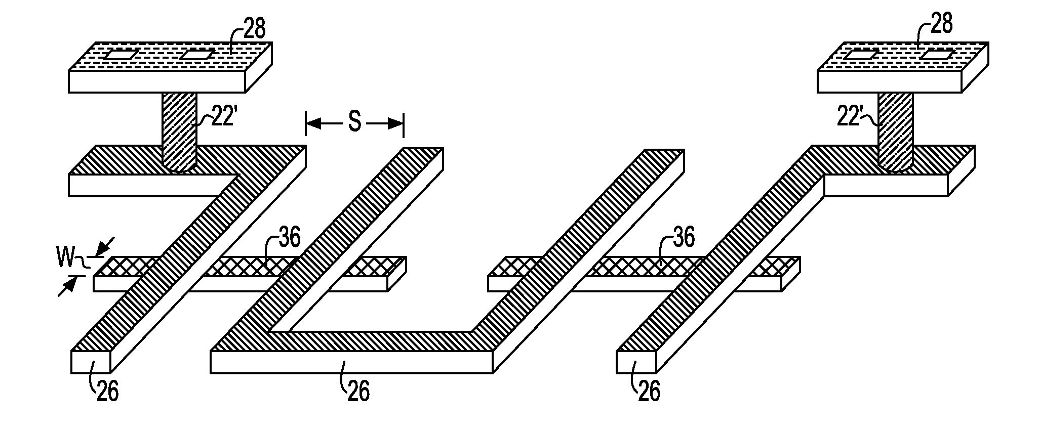
[0026]FIG. 1A to FIG. 12 show a series of schematic cross-sectional, plan-view and perspective-view diagrams illustrating the results of progressive stages in fabricating a contact resistance test structure within a three-dimensional integrated circuit structure (i.e., a microelectronic structure) in accordance with a particular embodiment of the invention. This particular embodiment of the invention comprises a particular sole preferred embodiment of the invention.

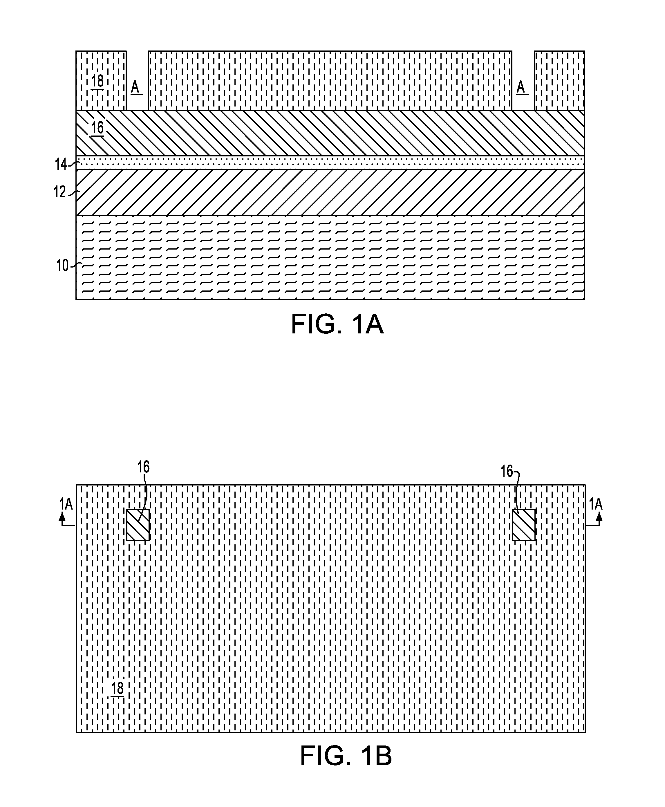
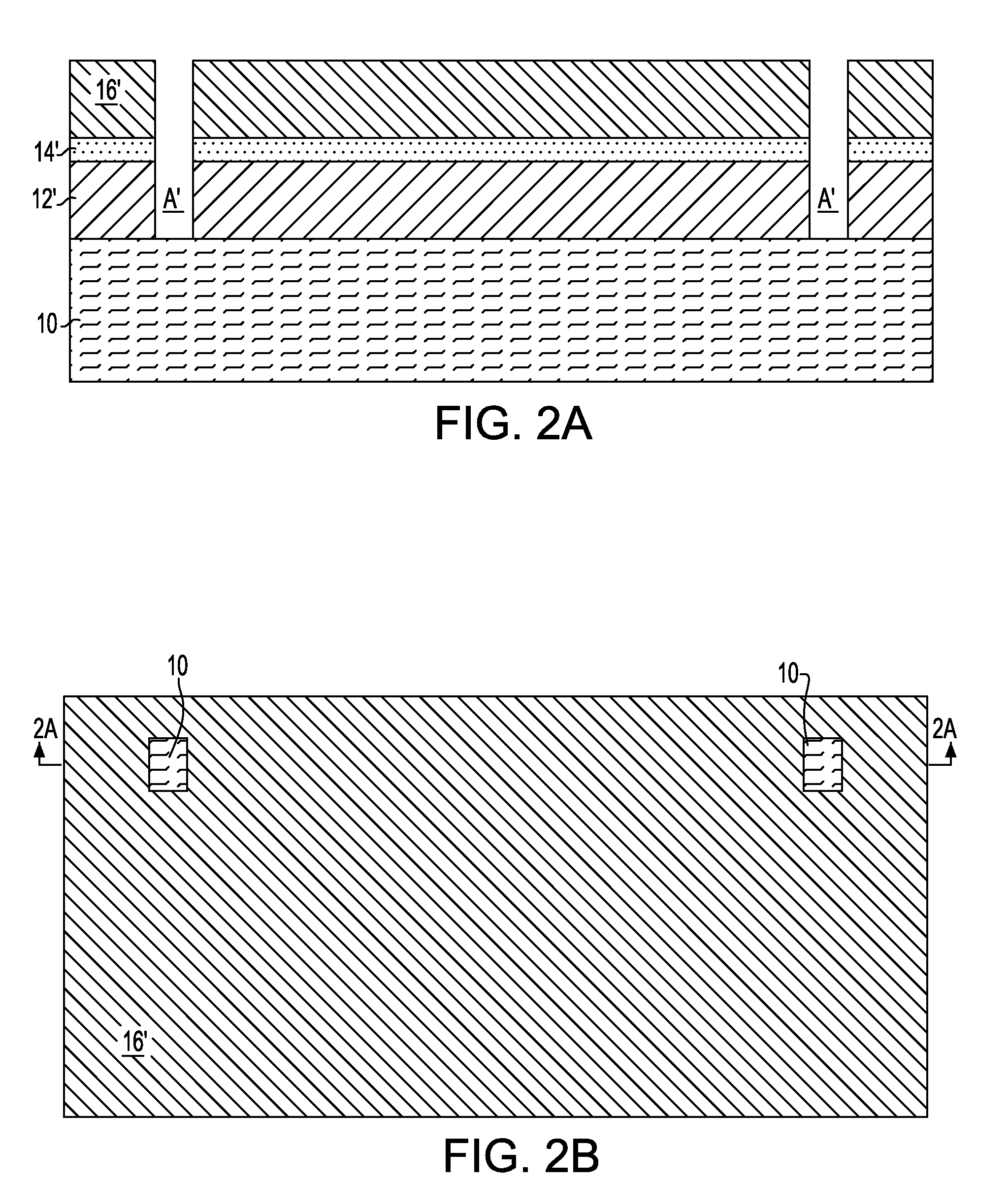
[0027]FIG. 1A and FIG. 1B show a schematic cross-sectio...


PUM


Abstract

A contact resistance test structure, a method for fabricating the contact resistance test structure and a method for measuring a contact resistance while using the contact resistance test structure are all predicated upon two parallel conductor lines (or multiples thereof) that are contacted by one perpendicular conductor line absent a via interposed there between. The test structure and related methods are applicable within the context of three-dimensional integrated circuits.

Description

[0001]This non-provisional application claims the benefit of the provisional application filed with the U.S. Patent and Trademark Office as Ser. No. 61 / 152,994 entitled “Contact Resistance Test Structure and Method Suitable for Three-Dimensional Integrated Circuits.BACKGROUND[0002]1. Field of the Invention[0003]The invention relates generally to microelectronic structures. More particularly, the invention relates to contact resistance test structures within microelectronic structures.[0004]2. Description of the Related Art[0005]As microelectronic structures and microelectronic devices have decreased in aerial plan-view dimensions to a point where aerial linewidth dimensions are nearing physical limitations of metal oxide semiconductor field effect transistor (MOSFET) scaling and lithographic capabilities, a trend has recently evolved within microelectronic fabrication, and in particular within semiconductor fabrication, to utilize a third vertical dimension when fabricating microele...

Claims


Application Information

Patent Timeline
IPC IPC(8): G01R31/26H01L23/58H01L21/768
CPCG01R31/2884H01L22/34G01R31/2601H01L21/76802G01R31/2851H01L2924/0002H01L22/14H01L2924/00
Inventor ZHU, HUILONG
Owner IBM CORP
Why Eureka
Try Eureka