
3-Axis Accelerometer With Gap-Closing Capacitive Electrodes

a capacitive electrode, three-axis technology, applied in the direction of speed/acceleration/shock measurement, measurement devices, instruments, etc., can solve the problems of non-differential sensing or complicated fabrication process, sensitivity is quite restrictive, and the fabrication process is complicated with high cos

Active Publication Date: 2010-08-26
NATIONAL TSING HUA UNIVERSITY
View PDF5 Cites 42 Cited by
  • Summary
  • Abstract
  • Description
  • Claims
  • Application Information

AI Technical Summary

Benefits of technology

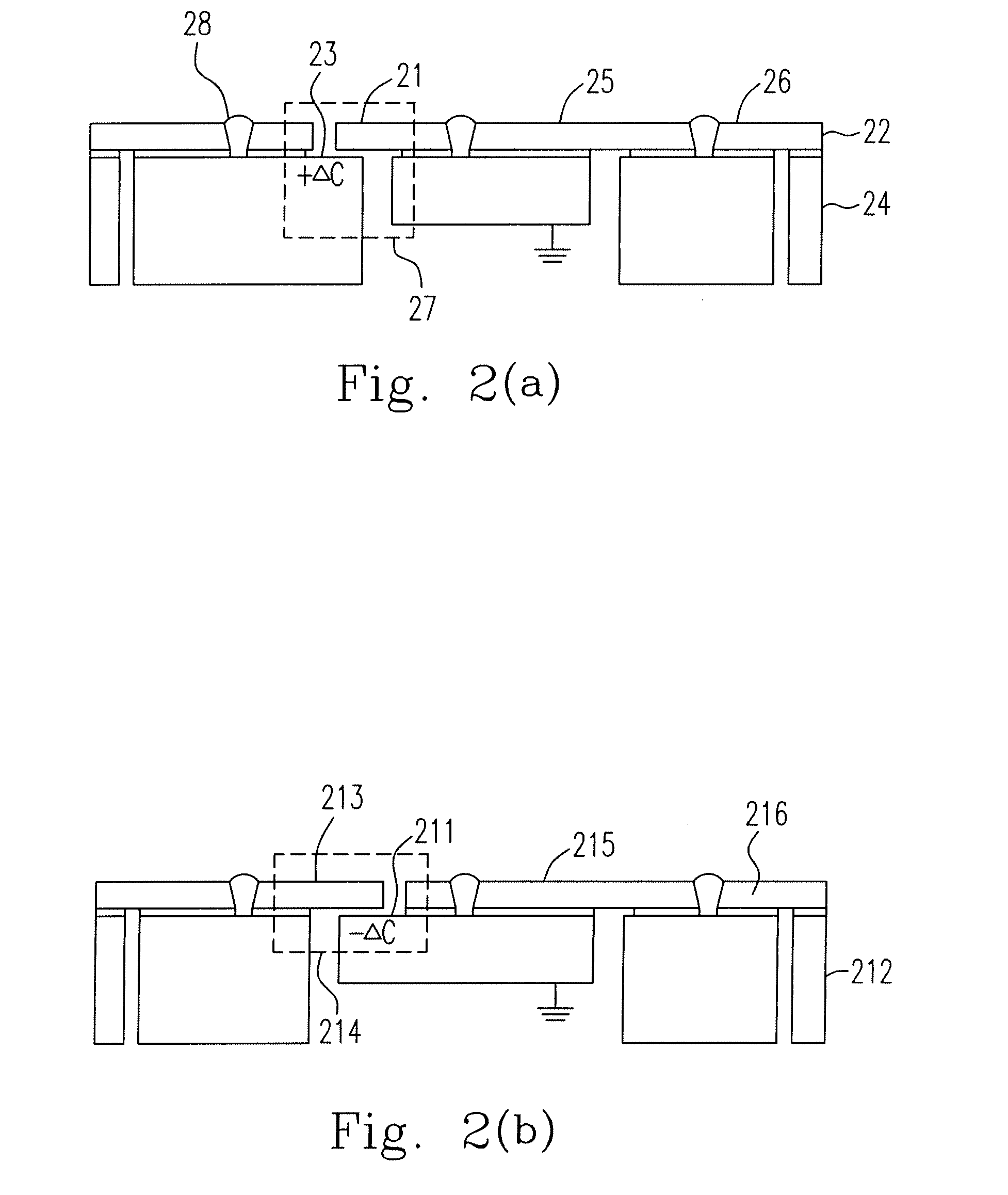
[0009]The main purpose of the present invention provides a gap closing differential capacitive sensing accelerometers on SOI wafer. The buried oxide layer thickness of SOI wafer is used for sensing gap, so the sensing gap could be precisely defined. The proof mass is consisted of device and handling layers, it could act either upper electrode or lower electrode. In addition, the present design of the sensing electrode arrays realizes the implementation of differential sensing circuit. The metal via like CMOS process is used to connect the device layer and handling layer to achieve differential sensing concept. The limit stop mechanism in this design is also considered, so the device could be protected in unexpected shock.

Problems solved by technology

However, the sensitivity is quite restrictive because of the area variation sensing scheme.
However, one of the main challenges for multi-axes accelerometer is how to detect the acceleration in the Z-axis (out-of-plane axis).
However, the fabrication process is complicated with high cost.
However, the electrode design in Z-axis is not the differential sensing architecture.
The above-mentioned researches suffer from either non-differential sensing or complicated fabrication processes in the Z-axis sensing.
However, Z-axis accelerometer with the gap closing differential electrodes using SOI wafer has still not yet been reported.

Method used


Image

  • 3-Axis Accelerometer With Gap-Closing Capacitive Electrodes
  • 3-Axis Accelerometer With Gap-Closing Capacitive Electrodes
  • 3-Axis Accelerometer With Gap-Closing Capacitive Electrodes

Examples


Embodiment Construction

[0036]The present invention will now be described more specifically with reference to the following embodiments. It is to be noted that the following descriptions of preferred embodiments of this invention are presented herein for the purposes of illustration and description only; it is not intended to be exhaustive or to be limited to the precise form disclosed.

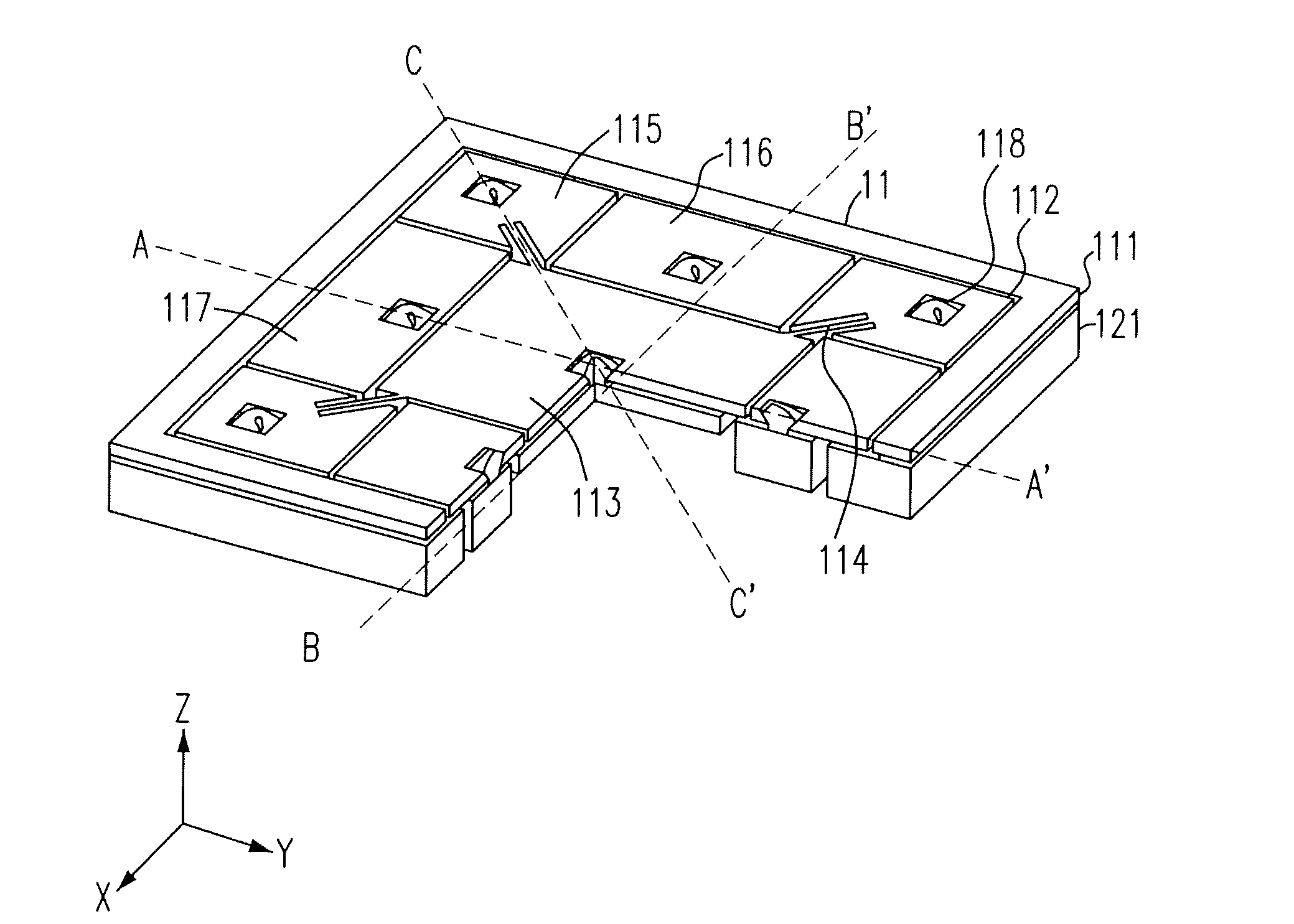
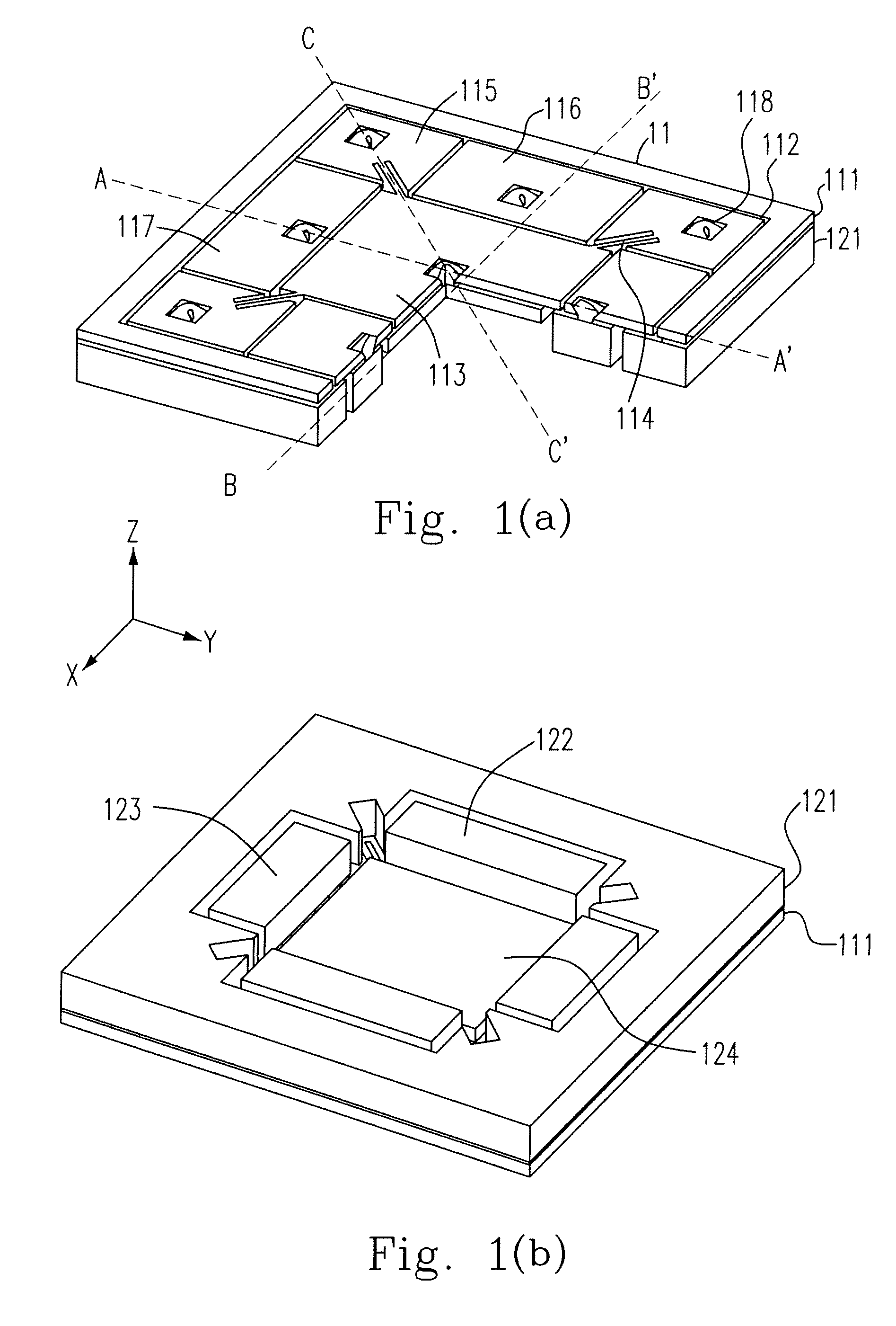
[0037]Please refer to FIG. 1(a), which is a front-side view showing a typical accelerometer of the present invention formed by the device silicon layer of SOI wafer. As indicated in FIG. 1(a), the device silicon layer 111 is partitioned into five regions electrically isolated to each other by trenches 112. For instance, the central proof-mass 113 together with the four springs 114 and their anchors 115 are connected and could be regarded as one electrical isolated region. The two rectangular areas 116 along the cross-section BB′ containing two upper stationary electrodes and their bonding pads are regarded as another two ele...


PUM


Abstract

Disclosed is a novel three-axis capacitive-type accelerometer implemented on SOI wafer. The accelerometer consists of four springs, one proof mass, four pairs of gap-closing sensing electrodes (each pair of gap-closing sensing electrode containing one movable electrode and one stationary electrode), and several metal-vias as the electrical interconnections. The movable electrodes are on the proof mass, whereas the stationary electrodes are fixed to the substrate. The three-axis accelerometer has five merits. (1) The sensitivity of the accelerometer is improved since the proof-mass is increased by containing both device and handling silicon layers; (2) The sensitivity is also improved by the gap-closing differential capacitive sensing electrodes design; (3) The parasitic capacitance at bond pad is reduced by the existing of metal-vias between the device Si layer and handling Si layer; (4) The sensing gap thickness is precisely defined by the buried oxide of SOI wafer; (5) The stationary sensing electrodes anchored to the substrate also act as the limit stops to protect the accelerometer.

Description

FIELD OF THE INVENTION[0001]The present invention relates to micro-electromechanical system accelerometer, and more particularly to a three-axis capacitive accelerometer.BACKGROUND OF THE INVENTION[0002]MEMS (Micro-electro-mechanical systems) accelerometer has been widely used in the automobile application, such as electronic stability control (ESC), adaptive cruise control (ACC), airbag systems and collision detection. The MEMS accelerometer even finds more applications in consumer electronics, for instance, the cell phone, PDA, digital still camera (DSC), and video games. Thus, the requirement of multi-axes accelerometer is rapidly increasing.[0003]Presently, a capacitive-based type sensing approach has been widely applied as an inertial sensor. There are several advantages for the capacitive-based type sensing approach. Capacitive-based techniques are inherently less noise than piezoresistance techniques because of the lack of thermal noises. In the differential capacitive sensin...

Claims


Application Information

Patent Timeline
IPC IPC(8): G01P15/125
CPCG01P15/0802G01P15/18G01P15/125
Inventor HSU, CHIA-PAOFANG, WEILEUNWU, MING-CHING
Owner NATIONAL TSING HUA UNIVERSITY
Learn More