Micro-electro-mechanical-system sensor and method for making same

a micro-electromechanical system and sensor technology, applied in the field of micro-electromechanical system (mems) sensors, can solve the problems of cmos process, equipment or materials which are not required, and process too complicated in the prior ar

Active Publication Date: 2010-08-26
PIXART IMAGING INC
View PDF8 Cites 16 Cited by
  • Summary
  • Abstract
  • Description
  • Claims
  • Application Information

AI Technical Summary

Benefits of technology

[0005]It is an objective of the present invention to provide a MEMS sensor which can be manufactured by a process fully compatible to the present standard CMOS process.

Problems solved by technology

U.S. Pat. No. 6,012,336; U.S. Pat. No. 6,536,281; U.S. Pat. No. 6,928,879; U.S. Pat. No. 7,121,146; U.S. Pat. No. 6,743,654; and U.S. Pat. No. 7,135,149 are relevant art, but the processes employed in these prior art either are too complicated or require equipment or materials which are not compatible to or not standard in CMOS process.

Method used


Image

  • Micro-electro-mechanical-system sensor and method for making same
  • Micro-electro-mechanical-system sensor and method for making same
  • Micro-electro-mechanical-system sensor and method for making same

Examples


Embodiment Construction

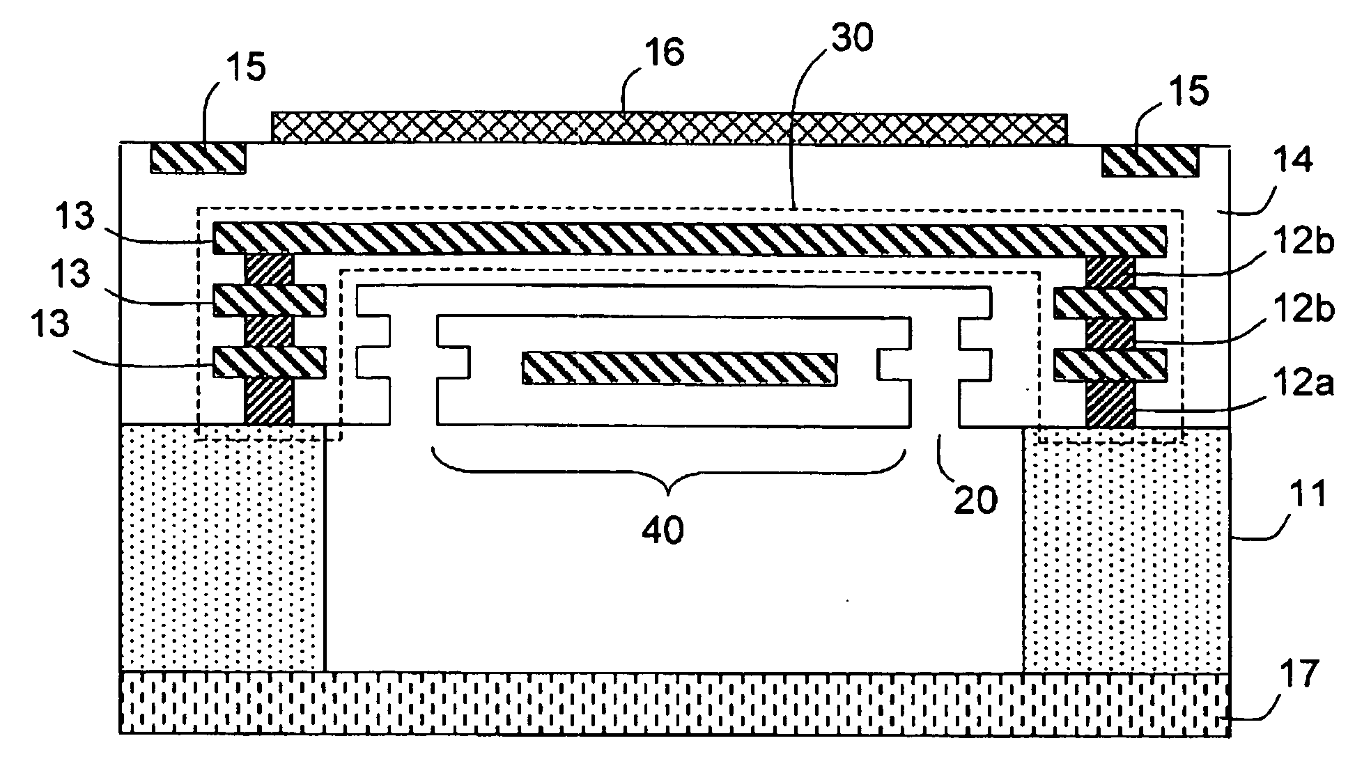
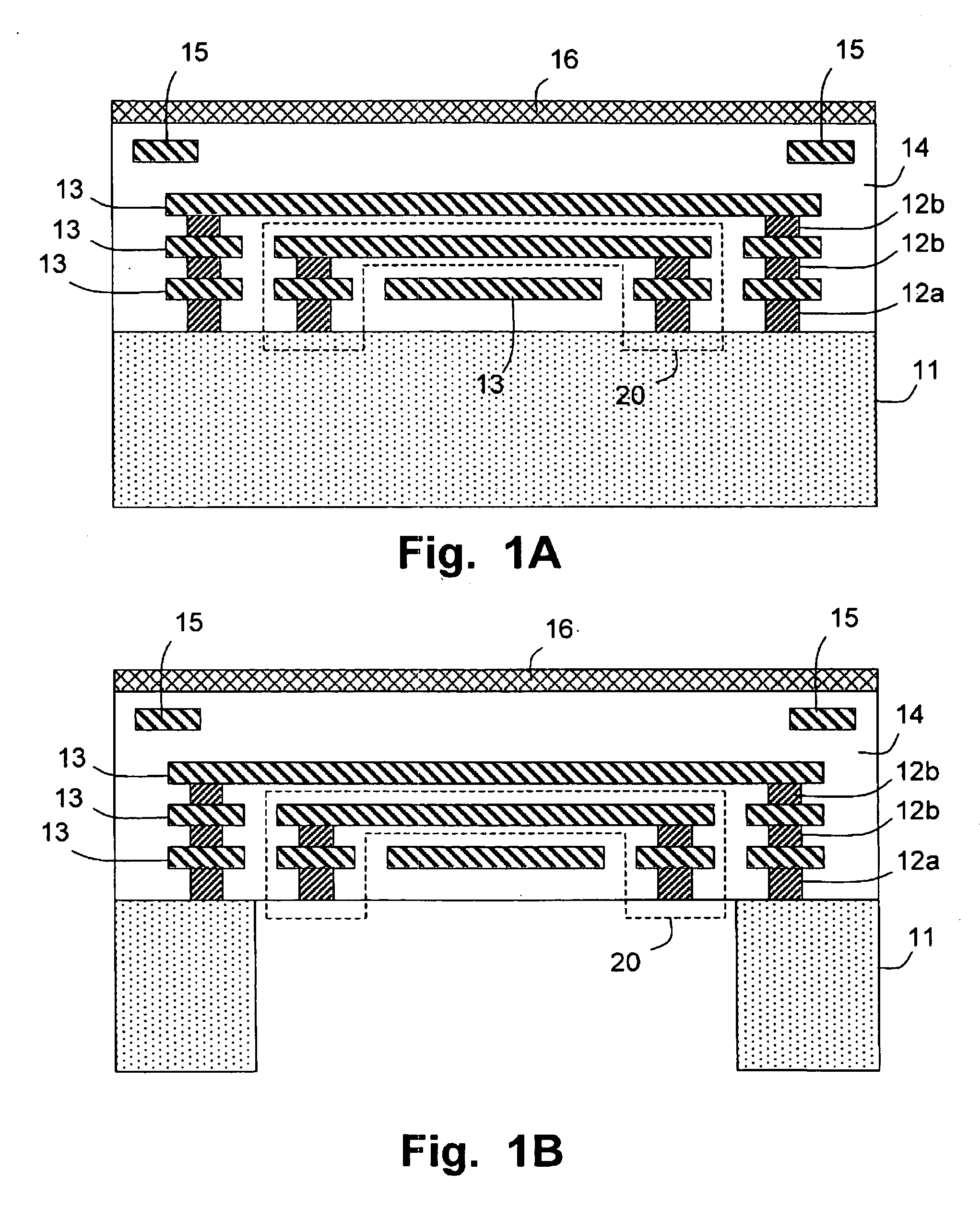
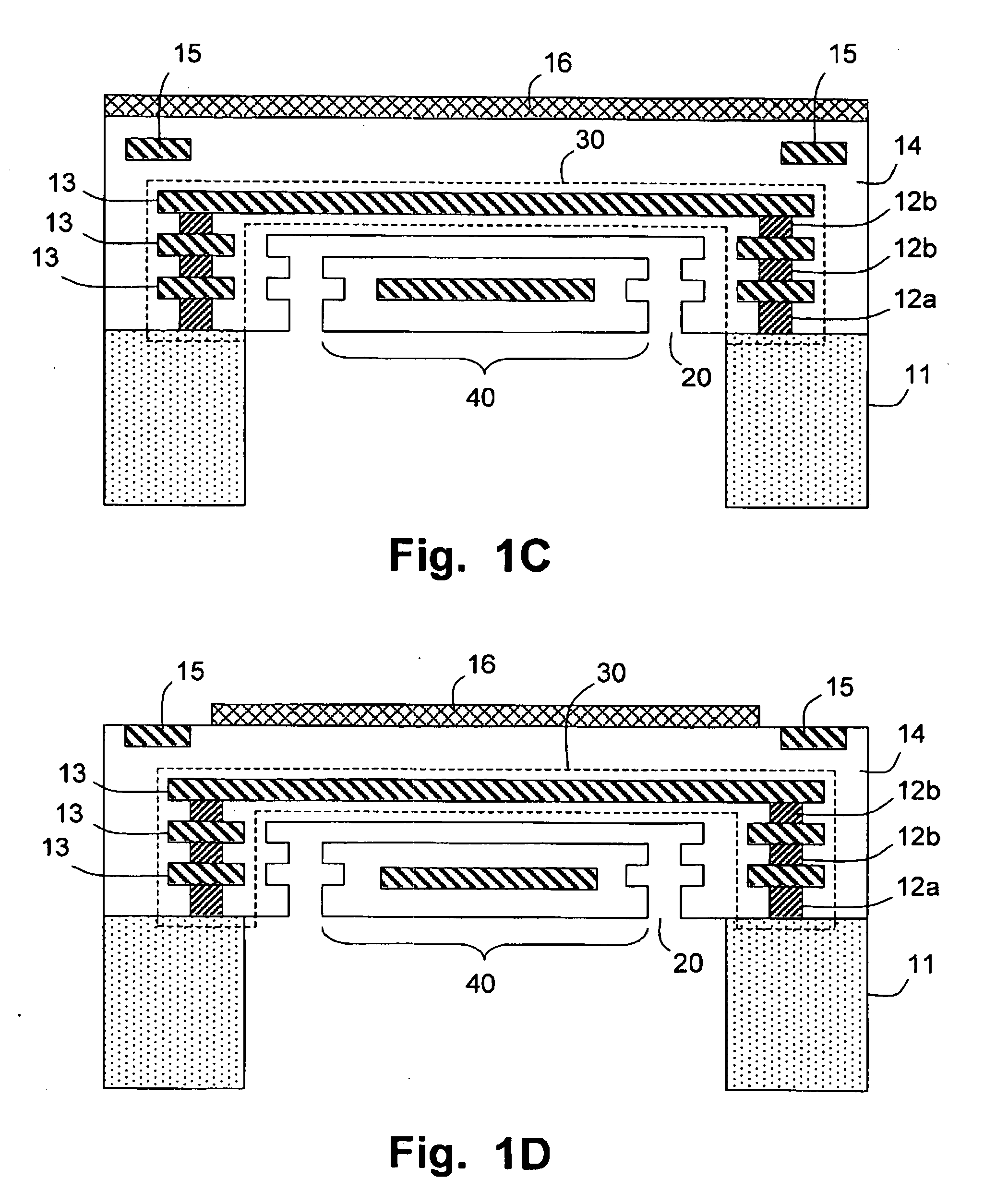
[0014]The drawings as referred to throughout the description of the present invention are for illustration only, but not drawn according to actual scale.

[0015]Referring to FIG. 1A for the first embodiment of the present invention, a zero-layer wafer substrate 11 is provided, which for example can be a silicon wafer so that the process is compatible with a standard CMOS process. Next, transistor devices can be formed by standard CMOS process steps as required (not shown), followed by deposition, lithography and etch steps to form interconnection including a contact layer 12a, metal layers 13, and via layers 12b. A dielectric layer 14 is provided to isolate the metal patterns of the layers where there should not be connection. Furthermore, a bond pad pattern 15 is formed on the topmost metal layer, and a passivation layer 16 is formed on top of the overall structure. In one embodiment, the contact layer 12a and the via layers 12b can be made of tungsten; the metal layers 13 can be mad...


PUM


Abstract

The present invention discloses an MEMS sensor and a method for making the MEMS sensor. The MEMS sensor according to the present invention comprises: a substrate including an opening; a suspended structure located above the opening; and an upper structure, a portion of which is at least partially separated from a portion of the suspended structure; wherein the suspended structure and the upper structure are separated from each other by a step including metal etch.

Description

BACKGROUND[0001]1. Field of Invention[0002]The present invention relates to a micro-electro-mechanical system (MEMS) sensor, in particular to a MEMS pressure sensor; the present invention also relates to a method for making such MEMS sensor, which is compatible to standard CMOS process.[0003]2. Description of Related Art[0004]MEMS devices are used in a wide variety of products; examples of such applications are absolute and relative sensors such as blood pressure sensor and micro-acoustical microphone. U.S. Pat. No. 6,012,336; U.S. Pat. No. 6,536,281; U.S. Pat. No. 6,928,879; U.S. Pat. No. 7,121,146; U.S. Pat. No. 6,743,654; and U.S. Pat. No. 7,135,149 are relevant art, but the processes employed in these prior art either are too complicated or require equipment or materials which are not compatible to or not standard in CMOS process. A MEMS sensor having a structure which can be manufactured by a standard CMOS process is desired in this industry.SUMMARY OF THE INVENTION[0005]It is ...

Claims


Application Information

Patent Timeline
Patent Type & Authority Applications(United States)
IPC IPC(8): H01L29/84H01L21/50
CPCB81B2201/0235B81C2203/0714B81C1/00246B81B2201/0257
Inventor WANG, CHUAN WEI
Owner PIXART IMAGING INC
Why Eureka
Try Eureka