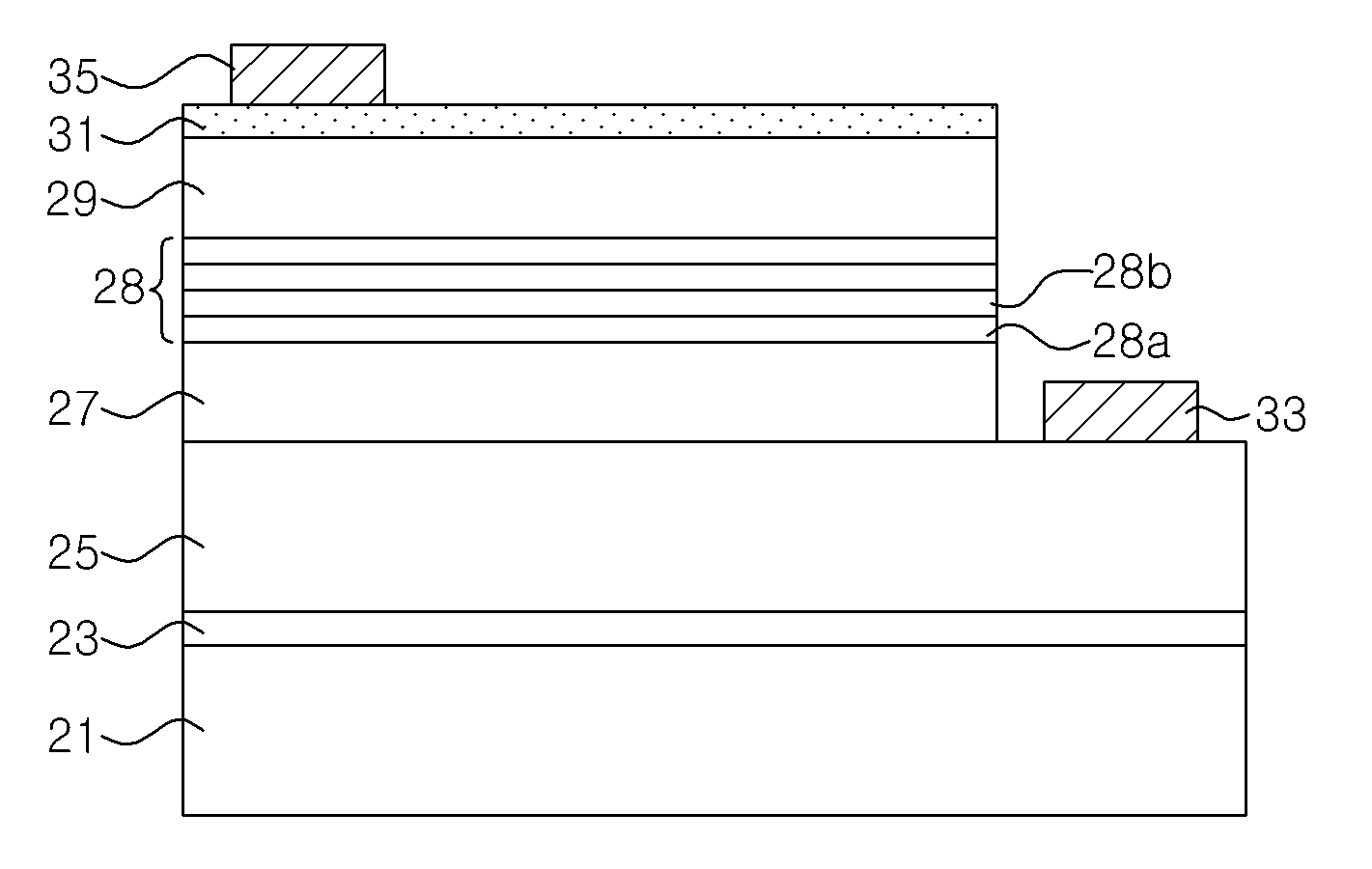
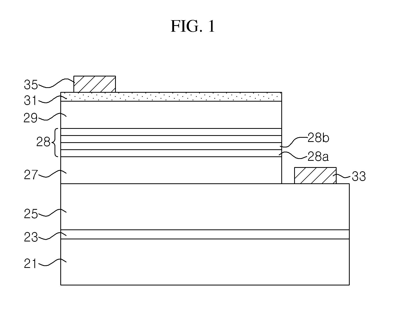
Light emitting device and method for manufacturing the same
a technology manufacturing methods, which is applied in the direction of semiconductor devices, lasers, semiconductor lasers, etc., can solve the problems of deterioration of reverse voltage characteristics, increase of current leakage, and lower current diffusion of light emitting devices, so as to improve electrical conductivity and/or crystallinity
- Summary
- Abstract
- Description
- Claims
- Application Information
AI Technical Summary
Benefits of technology
Problems solved by technology
Method used
Image

Examples
experiment 1
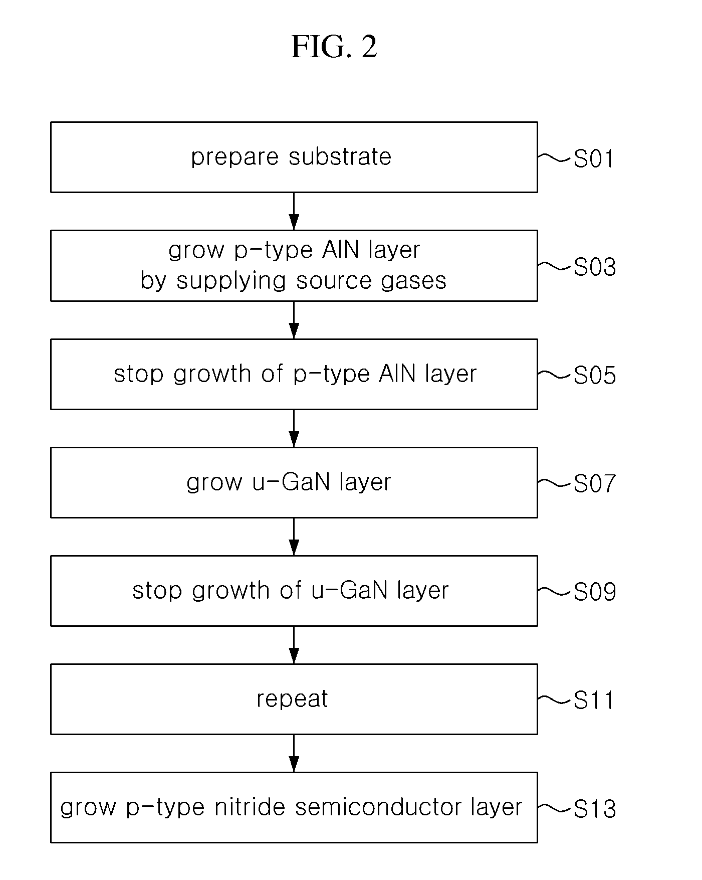
[0067
[0068]In Experiment 1, relationship between light emission and Mg flow during growth of p-type AlN / u-GaN layers constituting a super lattice structure was measured.
[0069]Temperature: 980° C.
[0070]Mg 120 sccm, 180 sccm, 240 sccm, 300 sccm, 360 sccm, 480 sccm
[0071]60 pairs of p-type AlN / u-GaN layers, time 0.1 min. / 0.1 min.
[0072]FIG. 4 is a graph depicting the relationship between light emission and Mg flow. As can be seen in FIG. 4, overall light emission was increased due to the use of the AlN / GaN layer of the super lattice structure. When growing the AlN / GaN layer, light emission was varied according to the Mg flow, and maximum light emission was obtained near 180 sccm of Mg.
experiment 2
[0073
[0074]In Experiment 2, relationship between light emission and Al flow during growth of p-type AlN / u-GaN layers constituting a super lattice structure was measured.
[0075]Temperature: 980° C.
[0076]Al: 32 / 40 / 31 (−10%); 40 / 40 / 31; 49 / 40 / 31 (+10%)
[0077]60 pairs of p-type AlN / u-GaN layers, time 0.1 min. / 0.1 min.
[0078]FIG. 5 is a graph depicting the relationship between light emission and Al flow. As can be seen in FIG. 5, overall light emission was increased due to the use of the AlN / GaN layer of the super lattice structure. When growing the AlN / GaN layer, the light emission was varied according to the Al flow, and maximum light emission was obtained near 40 sccm of Al.
[0079]The method of manufacturing the light emitting device according to the embodiment of the present invention can be applied to a light emitting diode and other nitride-based optical devices such as a laser diode and the like.
[0080]Although the present invention has been described with reference to exemplary embodim...
PUM
 Abstract
Description
Claims
Application Information