

Thin film transistor and method for producing the same
a technology of thin film transistors and manufacturing methods, applied in transistors, thermoelectric devices, nano-informatics, etc., can solve the problems of troublesome intersection part formation, difficult to form source electrodes and drain electrodes with uniform precision over a large substrate area, etc., to achieve suppressed deterioration, high precision, and suitable for increasing area
Active Publication Date: 2010-09-02
SONY CORP
View PDF12 Cites 34 Cited by
- Summary
- Abstract
- Description
- Claims
- Application Information
AI Technical Summary
Benefits of technology
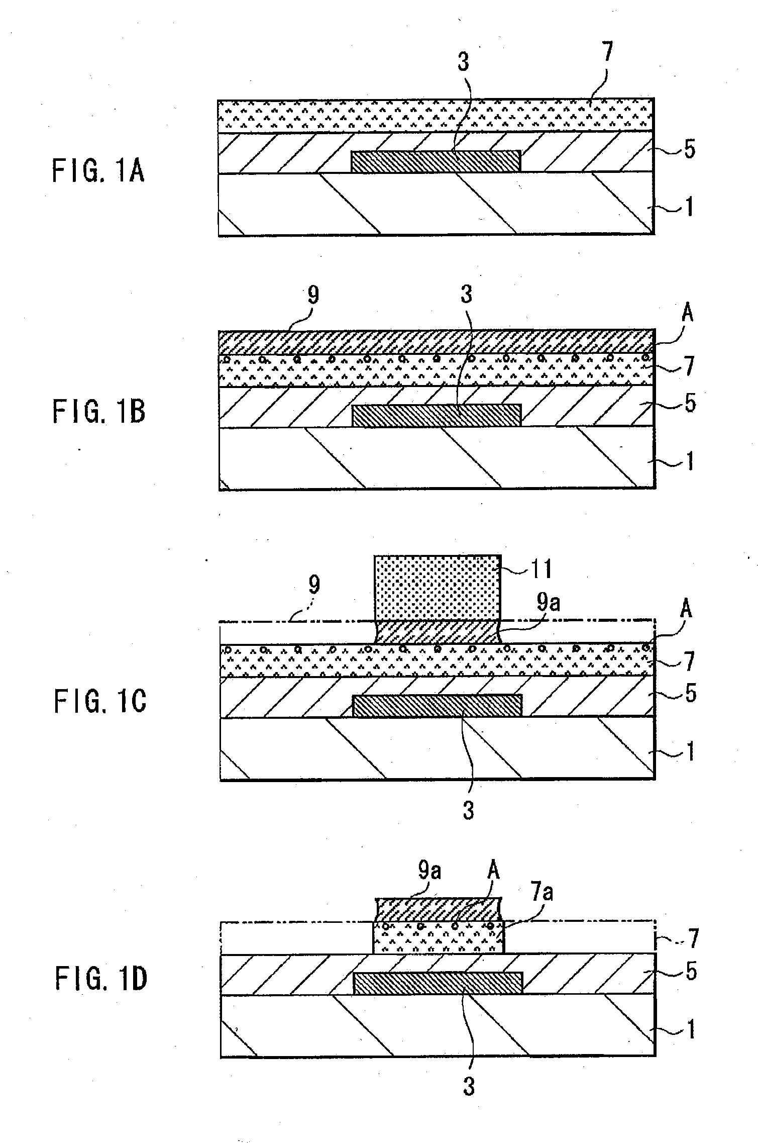
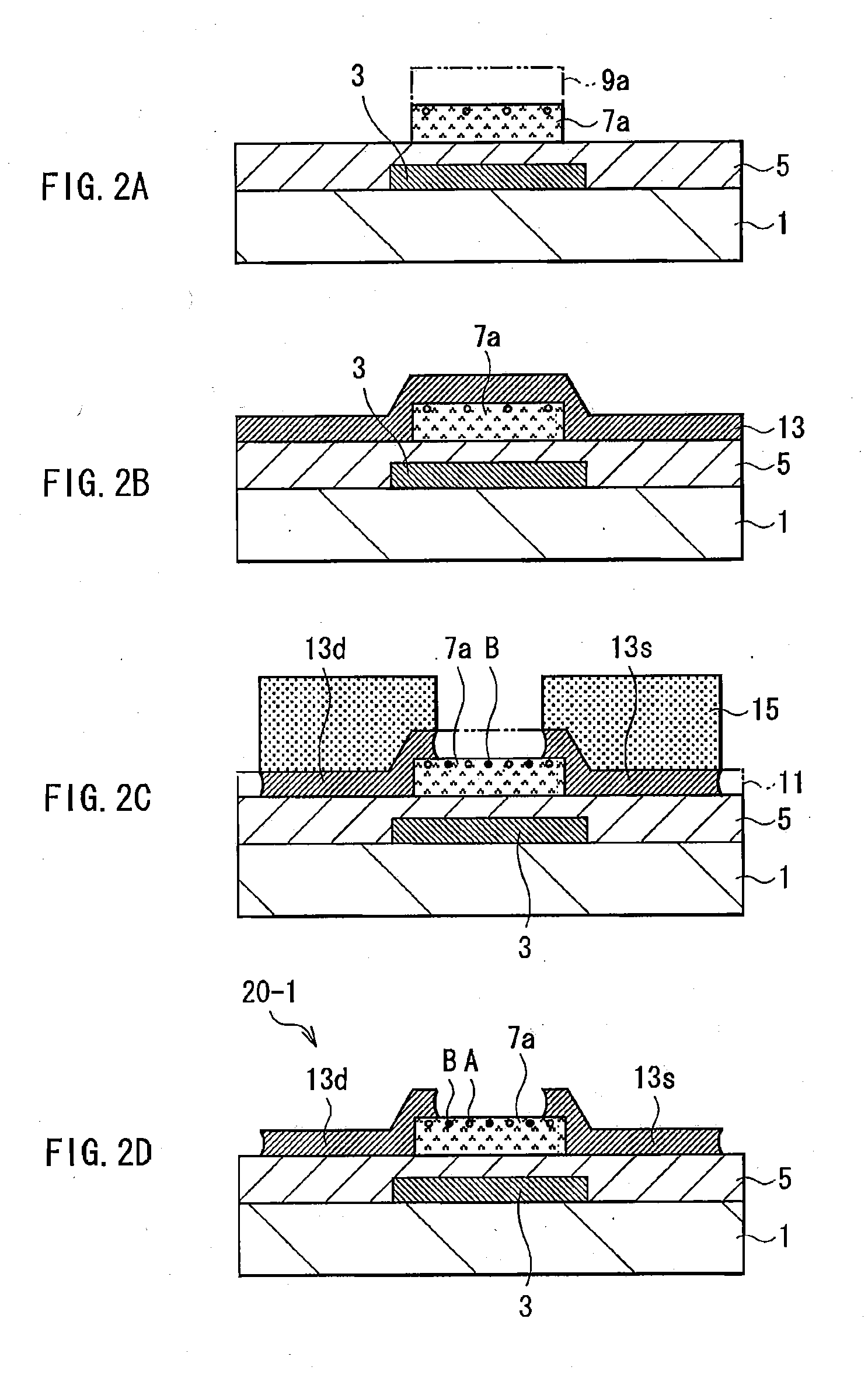
[0007]It is therefore desirable to provide a method of manufacturing a thin film transistor of a top-contact structure with suppressed deterioration by a process which is easy and suitable for increase in area without damaging an organic semiconductor pattern, a thin film transistor having a top-contact structure obtained by applying the method and, further, an electronic device having the thin film transistor.
[0010]In the method of manufacturing a thin film transistor, the electrode material film is etched using the resist pattern as a mask, so that the source electrode and the drain electrode patterned with high precision are formed. Since wet etching is performed as the etching of the electrode material film, the organic semiconductor layer under the electrode material film is prevented from being damaged. Further, since the etching process using the resist pattern as a mask is performed, the method is easy and suitable for increase in area.
[0012]According to a method of manufacturing a thin film transistor of an embodiment of the invention, while applying a process which is easy and suitable for increase in area, a thin film transistor of a top-contact structure with suppressed deterioration is obtained with high precision without damaging an organic semiconductor pattern. By using a thin film transistor obtained in such a manner, an electrode device with suppressed deterioration is obtained.
Problems solved by technology
However, in the manufacturing method using the intersecting part which halves a space above a substrate, formation of the intersection part is troublesome, and it is difficult to form a source electrode and a drain electrode with uniform precision over a substrate of large area.
Method used
View moreImage
Smart ImageViewing Examples

Examples
first embodiment (
1. First embodiment (method of manufacturing a thin film transistor)
second embodiment (
2. Second embodiment (an example of over-etching an organic semiconductor pattern)
third embodiment (
3. Third embodiment (an example of leaving a protection film pattern on an organic semiconductor pattern)
Login to View More PUM
| Property | Measurement | Unit |
|---|---|---|
| thickness | aaaaa | aaaaa |
| drain voltage | aaaaa | aaaaa |
| conductive | aaaaa | aaaaa |
Abstract
The present invention provides a method of manufacturing a thin film transistor of a top-contact structure with suppressed deterioration by a process which is easy and suitable for increase in area without damaging an organic semiconductor pattern. The organic semiconductor pattern is formed on a substrate. An electrode material film is formed on the substrate so as to cover the organic semiconductor pattern. A resist pattern is formed on the electrode material film. By wet etching using the resist pattern as a mask, the electrode material film is patterned. By the process, a source electrode and a drain electrode are formed.
Description
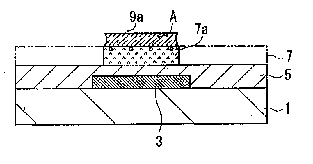
BACKGROUND OF THE INVENTION[0001]1. Field of the Invention[0002]The present invention relates to a method of manufacturing a thin film transistor, a thin film transistor, and an electronic device. More particularly, the invention relates to a method of manufacturing a thin film transistor in which fine source and drain electrodes are formed over an organic semiconductor pattern, a thin film transistor obtained by the method, and an electronic device using the thin film transistor.[0003]2. Description of the Related Art[0004]In recent years, attention is paid to a thin film transistor (TFT) using an organic semiconductor as a channel layer, a so-called organic TFT. Since the organic TFT is formed by applying a channel layer made of organic semiconductor at low temperature, it is advantageous to reduction of cost. The organic TFT is also formed on a flexible substrate having no heat resistance property such as a plastic substrate. It is known that, in an organic TFT having a top-conta...
Claims
Login to View More Application Information
Patent Timeline
 Patent Type & AuthorityApplications(United States)
IPC IPC(8): H01L51/10H01L51/40H01L29/772H10K99/00
CPCB82Y10/00H01L51/105H01L51/0011H01L51/0017H01L51/0021H01L51/0023H01L51/0035H01L51/0036H01L51/004H01L51/0046H01L51/0048H01L51/0052H01L51/0078H01L51/0545H01L51/102H01L27/3274H10K59/125H10K71/231H10K71/166H10K71/621H10K71/60H10K85/141H10K85/111H10K85/211H10K85/221H10K85/113H10K85/311H10K85/615H10K10/84H10K10/466H10K10/82
InventorKATSUHARA, MAOYONEYA, NOBUHIDE
OwnerSONY CORP