Oscillator based on series of four nanowires

Active Publication Date: 2010-09-02
COMMISSARIAT A LENERGIE ATOMIQUE ET AUX ENERGIES ALTERNATIVES
4 Cites 2 Cited by

AI-Extracted Technical Summary

Problems solved by technology

However, although obtaining a resonator of reasonable size is an important point, in order to transform a resonator into an oscillator, the electronic part that is ...

Method used

[0024]The use of at least one additional series of four sub-assemblies 1 enables the transductance gain to be increased so as to comply with the global oscillation condition of resonators 4.
[0031]It is advantageous to use the first alternative embodiment instead of the second alternative embodiment as the first alternative embodiment uses less r...

Benefits of technology

[0006]The object of the invention is to provide an oscillat...

Abstract

The oscillator comprises at least a first series of a multiple of four sub-assemblies each of which comprises an excitation terminal and an output terminal. The sub-assemblies are arranged in series in a closed loop. The output terminal of each sub-assembly is connected to the excitation terminal of the following sub-assembly. The output terminal of one of the sub-assemblies constitutes the output terminal of the oscillator. Each sub-assembly comprises excitation means and a nanowire which constitutes the electromechanical resonator and the piezoresistive detection means of movement of the resonator. A first terminal of the nanowire is connected to a first supply voltage. The second terminal of the nanowire constitutes the output terminal of the sub-assembly which is grounded via a corresponding resistive circuit. An input terminal of the excitation means constitutes the excitation terminal of the sub-assembly.

Application Domain

Pulse generation by logic circuitsOscillations generators

Technology Topic

PhysicsResonator +4

Image

  • Oscillator based on series of four nanowires
  • Oscillator based on series of four nanowires
  • Oscillator based on series of four nanowires

Examples

  • Experimental program(1)

Example

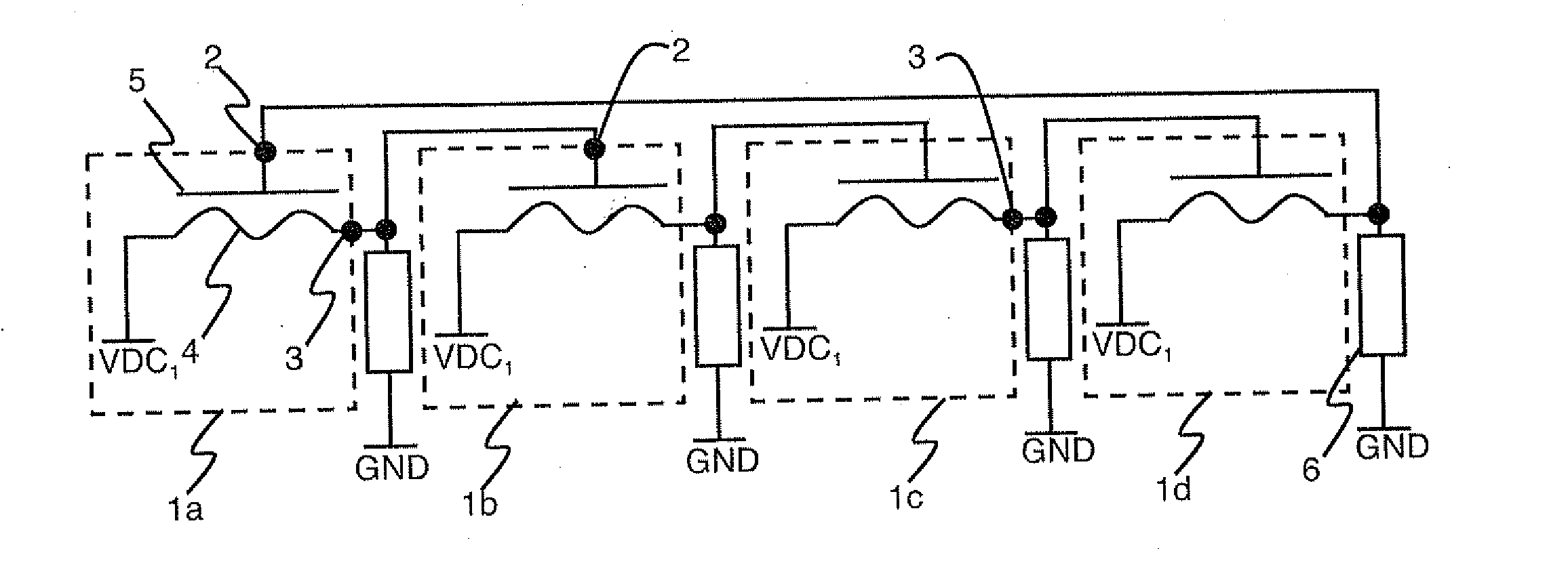
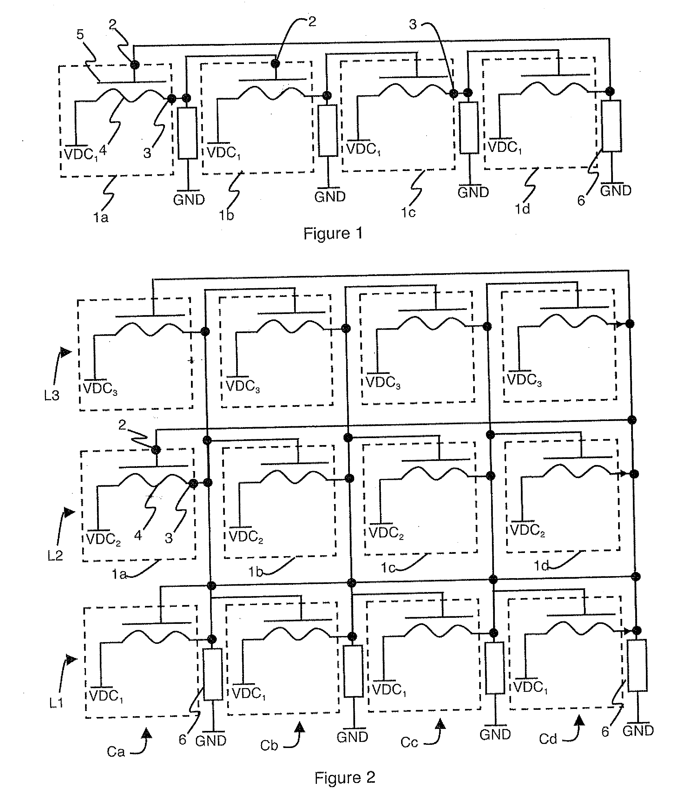
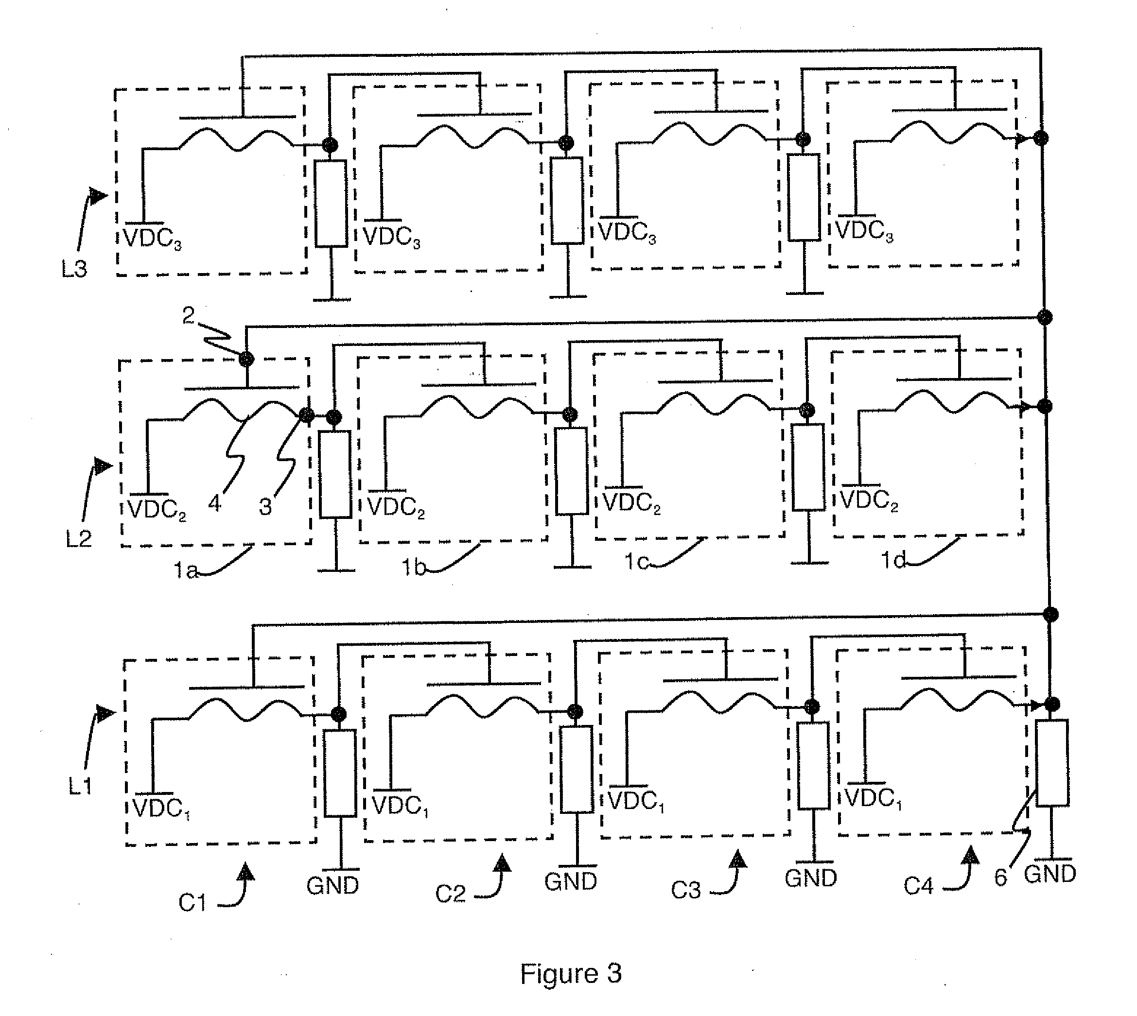
[0013]As illustrated in FIG. 1, the oscillator comprises a first series of four sub-assemblies 1 (1a, 1b, 1c and 1d) which are connected together in series to form a closed loop. Each sub-assembly 1 of the first series comprises an excitation terminal 2 and an output terminal 3 and is connected to two other adjacent sub-assemblies 1. if the first series is considered to comprise first 1a, second 1b, third 1c and fourth 1d sub-assemblies, second sub-assembly 1b is connected to first sub-assembly 1a and to third sub-assembly 1c. Third sub-assembly 1c is also connected to fourth sub-assembly 1d which is itself connected to first sub-assembly 1a.
[0014]Each sub-assembly 1 comprises a resonator 4, excitation means 5 of the resonator and detection means of movement of the resonator. In each sub-assembly 1, a nanowire 4 constitutes an electromechanical resonator. Movement of the nanowire 4 is converted into a representative electric signal by a suitable transductance means formed by the detection means of the sub-assembly. The detection means are advantageously of piezoresistive type and are formed directly by nanowire 4 which presents a giant piezo-resistance effect as is described in the article by He et al. (“Giant piezoresistance effect in silicon nanowires” Nature nanotechnology, vol. 1, October 2006, pp 42-46). Each sub-assembly 1 therefore comprises excitation means 5 of nanowire 4. Each sub-assembly comprises at least one nanowire, i.e. a nanowire as in the embodiments illustrated in FIGS. 1 to 3, or a plurality of nanowires as in the embodiments illustrated in FIGS. 4 and 5.
[0015]In each sub-assembly 1 of the first series, a first terminal of nanowire 4 is connected to a first supply voltage (VDC1), and a second terminal of nanowire 4 constitutes output terminal 3 of sub-assembly 1. An input terminal of excitation means 5 constitutes excitation terminal 2 of sub-assembly 1. Output terminal 3 of each sub-assembly 1 is connected to ground GND by means of a corresponding resistive circuit 6.
[0016]To form a closed loop, output terminal 3 of each sub-assembly 1 is connected to excitation terminal 2 of the following sub-assembly 1. The direction of data transit in a sub-assembly 1 is thus considered to be from an excitation terminal 2 to an output terminal 3. The oscillator comprises an output terminal which is formed by output terminal 3 of one of sub-assemblies 1. The oscillator also comprises an input terminal which is formed by excitation terminal 2 of the sub-assembly which follows the sub-assembly comprising the output terminal of the oscillator.
[0017]Resistive circuit 6 can be formed by a resistor, a field-effect or bipolar transistor, a resistive bridge or any other component capable of converting a current variation into a voltage variation.
[0018]For example purposes, if the output terminal of the signal representative of the oscillator is formed by output terminal 3 of fourth sub-assembly 1d, the input terminal of an electric signal in the oscillator is formed by excitation terminal 2 of first sub-assembly 1a.
[0019]In this way, each sub-assembly 1 transmits a signal representative of the movement of its nanowire 4 to excitation means 5 of the following sub-assembly 1 which controls actuation of the following nanowire 4. The voltage at the terminals of resistive circuit 6 associated with the output terminal of the oscillator, here resistive circuit 6 associated with fourth sub-assembly 1d, is representative of the current delivered by fourth nanowire 4. The signal emitted by the detection means is converted into a voltage by means of resistive circuit 6 to generate an actuating force on the following nanowire 4 and to thereby fulfil the oscillation conditions.
[0020]The dynamics of the four nanowires 4 of the first series enable the phase condition necessary for obtaining an oscillator to be fulfilled without an external phase-shift element being added. Moreover, the giant piezo-resistance effect observed in the nanowires enables gain values necessary for triggering oscillation to be achieved. Each sub-assembly performing a 90° phase shift, the use of a first series of four sub-assemblies 1 results in a global phase shift of 0° necessary to maintain the oscillations of the resonators in the oscillator. It is also conceivable to produce an oscillator comprising a multiple of four sub-assemblies 1 in order to obtain a global phase shift of 0°. The first series of sub-assemblies can therefore for example contain four, eight, twelve, sixteen or more sub-assemblies.
[0021]Excitation of each nanowire 4 is performed independently by excitation means 5 of capacitive or magnetic, or possibly thermal, type. In the case of capacitive excitation, the electrostatic force of excitation means 5 is obtained by means of the voltage difference that exists between supply voltage VDC applied to nanowire 4 (a DC voltage) and the output voltage of the detection means of the previous sub-assembly 1 (an AC voltage). The output voltage of the detection means of the previous sub-assembly 1 is applied to an electrode of the excitation means. Use of magnetic excitation means has been described by Feng et al. “Very High Frequency Silicon Nanowire Electromechanical Resonators” Nano Letters 2007, Vol. 7, N° 7. pp 1953-1957.
[0022]If the gain of the piezoresistive transductance performed by nanowires 4 is insufficient, it is advantageous to use at least one additional series of four sub-assemblies 1 (FIGS. 2 and 3). These sub-assemblies are identical in their construction to those of the first series. In the additional series, the nanowires are connected to a specific additional supply voltage VDCn.
[0023]In a particular embodiment, additional supply voltage VDCn is identical to first supply voltage VDC1.
[0024]The use of at least one additional series of four sub-assemblies 1 enables the transductance gain to be increased so as to comply with the global oscillation condition of resonators 4.
[0025]In a particular use, adjustment of supply voltage VDC of the different series of sub-assemblies enables a voltage-controlled oscillator to be obtained.
[0026]In a first alternative embodiment illustrated in FIG. 2, a plurality of additional series each comprising four sub-assemblies 1 is integrated in the oscillator.
[0027]in this alternative embodiment, a sub-assembly 1 of each additional series is connected in parallel to excitation terminal 2 and output terminal 3 of a corresponding sub-assembly 1 of the first series. This results in the oscillator comprising four columns (Ca, Cb, Cc and Cd) of sub-assemblies 1 and in all the columns presenting the same number of sub-assemblies 1. Thus, schematically, all the excitation terminals 2 of the sub-assemblies of any one column are connected to the same electric point, as they all receive the same signal, i.e. the same voltage. The same is the case for all the output terminals 3 of sub-assemblies 1 of any one column. The currents supplied by the nanowires of any one column in fact create a voltage at the terminals of resistive circuit 6 associated with this column that is representative of the sum of the supplied currents. This output voltage is then applied to all the excitation means 5 of the next column. In the particular embodiment of FIG. 2, only three series of sub-assemblies are illustrated, each series having its own supply voltage VDC1, VDC2, VDC3. Each series is represented in FIG. 2 by a line (L1, L2 and L3) of sub-assemblies that in addition comprises its own supply voltage.
[0028]In a second alternative embodiment illustrated in FIG. 3, a plurality of additional series each comprising four sub-assemblies 1a, 1b, 1c and 1d is also integrated in the oscillator. In each additional series, connection of the sub-assemblies 1 to one another is substantially identical to that of the first series. Output terminal 3 of three consecutive sub-assemblies is connected to ground GND via a corresponding resistive circuit 6. Each series is represented in FIG. 3 by a line (L1, L2 and L3) of sub-assemblies which in addition comprises its own supply voltage.
[0029]Thus, output terminal 3 of one of the sub-assemblies being connected to the output terminal of the oscillator, output terminals 3 of the sub-assemblies of the additional series that are not connected to the output of the oscillator are connected to GND via a corresponding resistive circuit 6. In the example illustrated in FIG. 3, first, second and third sub-assemblies 1 are grounded via their output terminal 3 and via a resistive circuit 6 whereas output terminal 3 of fourth sub-assembly 1d is connected directly to output terminal 3 of the fourth sub-assembly of the first series. As in the previous embodiment, FIG. 3 only illustrates a particular embodiment comprising three series of sub-assemblies having their own supply voltage VDCn.
[0030]In this embodiment, as in the previous embodiment, the voltage at the terminals of resistive circuit 6 associated with the output terminal of the oscillator is representative of the sum of the currents provided by the plurality of series of sub-assemblies (the first series and the additional series). The transductance gain of the nanowires is therefore multiplied by the number of series of sub-assemblies integrated in the oscillator.
[0031]It is advantageous to use the first alternative embodiment instead of the second alternative embodiment as the first alternative embodiment uses less resistive circuits thereby enabling the surface area used to be reduced.
[0032]Nanowires 4 that form the resonators and detection means can present a square, rectangular or circular cross-section. The dimensions of the nanowire in this cross-section are typically smaller than 100 nm, for example between 10 and 40 nm. For example, if the diameter of the nanowire is equal to 10 nm and the length is equal to 1.15 μm, the resonance frequency has to be equal to 50 MHz. if its length is equal to 600 nm, the resonance frequency is then equal to 200 MHz. If the nanowire has a square cross-section, a thickness equal to 20 nm and a length equal to 1.30 μm, the resonance frequency is equal to 100 MHz. If the thickness is equal to 40 nm and the length is equal to 1.90 μm, the resonance frequency is equal to 100 MHz.
[0033]Advantageously, the equivalent resistance of resistive circuit 6 is chosen equal to the static resistance of nanowire 4 with which this circuit is associated. In a particular embodiment, resistive circuit 6 is formed by a resistance, and in an even more particular embodiment, the resistance constituting the resistive circuit is formed by a nanowire identical to that of the associated sub-assembly but which is not released from its support substrate to prevent oscillation thereof—the nanowire is said to be fixed. Resistive circuit 6 can also be a transistor that is used as a resistance.
[0034]It is also possible to adjust the value of the equivalent resistance of the resistive circuit in order to reduce the current leakage originating from the nanowires which also has the effect of modifying the value of the gain linked to the transductance by the nanowires.
[0035]The nanowires are made from electrically conducting materials, for example from semi-conducting materials such as silicon, germanium or silicon-germanium alloys. For nanowires made from semi-conducting material, doping has to be performed. Typically, for a silicon nanowire, a doping equal to 1019 cm−3 (with boron) enables a transductance gain of more than one to be obtained. If a weaker doping level is used, as the static resistance of the nanowire is increasing, it may be necessary to provide additional series of sub-assemblies.
[0036]For example purposes, for doping of silicon nanowires of about 1017 cm−3 (with boron), about ten additional series of sub-assemblies have to be used. For doping of about 1016 cm−3, about a hundred additional series may be required.
[0037]In the embodiment illustrated in FIG. 2, when several series of sub-assemblies 1 are integrated in a single oscillator, the different excitation means 5 of any one column all receive the same signal. They all actuate nanowires 4 in the same way. As illustrated in FIGS. 4 and 5, it is advantageous to arrange the nanowires in a two-dimensional or three-dimensional network and to use an excitation means 5 common to all the nanowires 4 of any one column. The nanowires of any one column can then be addressed collectively, for example by means of a series of metal tracks or doped areas at the surface or by a network of three-dimensional metal interconnections. In this case, excitation terminal 2 and output terminal 3 of the different sub-assemblies 1 of any one column are physically one and the same, as there is one sub-assembly associated with each nanowire.
[0038]For example purposes, the nanowire or nanowires of any one column are formed on a SOI substrate and are resting for example on the buried oxide. The nanowires are for example formed by photolithography and etching or by chemical vapor deposition. The buried oxide is then removed in controlled manner underneath a part of the nanowires in order to make movement of the latter possible. The nanowires are then suspended above the substrate situated under the buried oxide and application of a variable voltage between the nanowire and substrate enables the excitation means to apply electrostatic forces capable of making the nanowire resonate.
[0039]Thus, in each sub-assembly, excitation means 5 comprise at least one electrode which is arranged facing the nanowire or nanowires. The electrode or electrodes are then connected to the excitation terminal of the excitation means of the sub-assembly.
[0040]In the oscillator, there is no feedback loop formed by an electronic circuit which enables an extremely compact, purely electromechanical oscillator to be achieved. The only power input to the oscillator is performed by supply voltage VDC which is a DC voltage applied on each nanowire. Supply voltage VDC enables the amplitude of the oscillations of the nanowires to be controlled.

PUM

no PUM

Description & Claims & Application Information

We can also present the details of the Description, Claims and Application information to help users get a comprehensive understanding of the technical details of the patent, such as background art, summary of invention, brief description of drawings, description of embodiments, and other original content. On the other hand, users can also determine the specific scope of protection of the technology through the list of claims; as well as understand the changes in the life cycle of the technology with the presentation of the patent timeline. Login to view more.

Similar technology patents

Compact folding seat

ActiveUS20050264065A1extremely compacteasy to operate
Owner:DIONO

Hinge retarding device such as for vehicle glove compartment lids

InactiveUS7043797B2straightforward to produceextremely compact
Owner:ITW FASTEX ITALIA SPA

Message speed limit method

ActiveCN1725732Aeasy to implementTake up less resources
Owner:NEW H3C TECH CO LTD

Classification and recommendation of technical efficacy words

  • easy to implement
  • extremely compact

Intelligent video monitoring method and system thereof

InactiveCN101635835AEasy to implementEasy system expansion
Owner:SHENZHEN XINYI TECH CO LTD

Voice call routing by dynamic personal profile

InactiveUS7653191B1less laboreasy to implement
Owner:MICROSOFT TECH LICENSING LLC

Compact folding seat

ActiveUS20050264065A1extremely compacteasy to operate
Owner:DIONO

Hinge retarding device such as for vehicle glove compartment lids

InactiveUS7043797B2straightforward to produceextremely compact
Owner:ITW FASTEX ITALIA SPA
Why Eureka
Try Eureka