Antenna device

a technology of antenna and input impedance, which is applied in the direction of resonant antennas, antenna earthings, elongated active element feeds, etc., can solve the problems of limiting the adjustable impedance range, antenna cannot exhibit the performance inherent in the antenna, and the vswr characteristics of the antenna deteriorate, so as to achieve easy adjustment, easy adjustment of input impedance, and convenient adjustment of inductan

Inactive Publication Date: 2010-09-02
TDK CORPARATION
View PDF9 Cites 17 Cited by
  • Summary
  • Abstract
  • Description
  • Claims
  • Application Information

AI Technical Summary

Benefits of technology

[0007]Therefore, the object of the present invention is to provide an antenna device that does not have a particular structure such as a trio-land structure, that is capable of efficiently generating an electromagnetic field between the conductor pattern formed on the surface of a base made of a dielectric material and the ground pattern surrounding the conductor pattern, facilitates resonance frequency adjustment and input impedance adjustment, and accordingly, is capable of improving its antenna characteristics.

Problems solved by technology

When the input impedance does not match a feeder-side impedance, VSWR characteristics of the antenna deteriorate and the antenna cannot exhibit performance inherent in the antenna.
As a result, there is a limit to the adjustable impedance range.

Method used


Image

  • Antenna device
  • Antenna device
  • Antenna device

Examples


example 1

[0068]The antenna characteristics were measured while the position of the antenna mounting region was changed on the printed circuit board. The size of the printed circuit board was 80 mm×37 mm×1 mm, the size of the antenna mounting region was 3.0 mm×4.5 mm, and the chip size of the antenna element was 2.0 mm×1.2 mm×1.0 mm. As shown in FIG. 10, a sample S1 has the antenna mounting region located at the position of 50% from the reference point of the circuit board or at a corner portion of the circuit board, a sample S2 has the antenna mounting region located at the reference point (0%) of the circuit board, a sample S3 has the antenna mounting region located at the position of 25% from the reference point of the circuit board or at the mid point between the reference point and a corner portion, and a sample S4 has the antenna mounting region located at the position of 37.5% from the reference point of the circuit board or at the mid point between the antenna mounting region of the s...

example 2

[0071]The antenna characteristics were measured while the aspect ratio of the antenna mounting region was varied. The size of the printed circuit board was 80 mm×37 mm×1 mm, and the antenna mounting region was located at the reference point (0%) in the longitudinal direction of the printed circuit board. The size (Wa×Wb, as shown in FIG. 5A) of the antenna mounting region was 3 mm×5 mm in a sample S5, 3 mm×4.5 mm in a sample S6, and 3 mm×4 mm in a sample S7. The chip size of the antenna element was 2.0 mm×1.2 mm×1.0 mm, and the relative permittivity ∈r of the base of the antenna element was 37. The conductor patterns on the antenna element were adjusted so that the resonance frequency of each of the samples S5 to S7 became 2.43 GHz, and the input impedance became 50Ω. After that, signals between 2.3 GHz to 2.6 GHz were supplied through a signal line with the use of a network analyzer, and the return loss and radiation efficiency of the antenna device were measured. FIGS. 12A and 12B...


PUM


Abstract

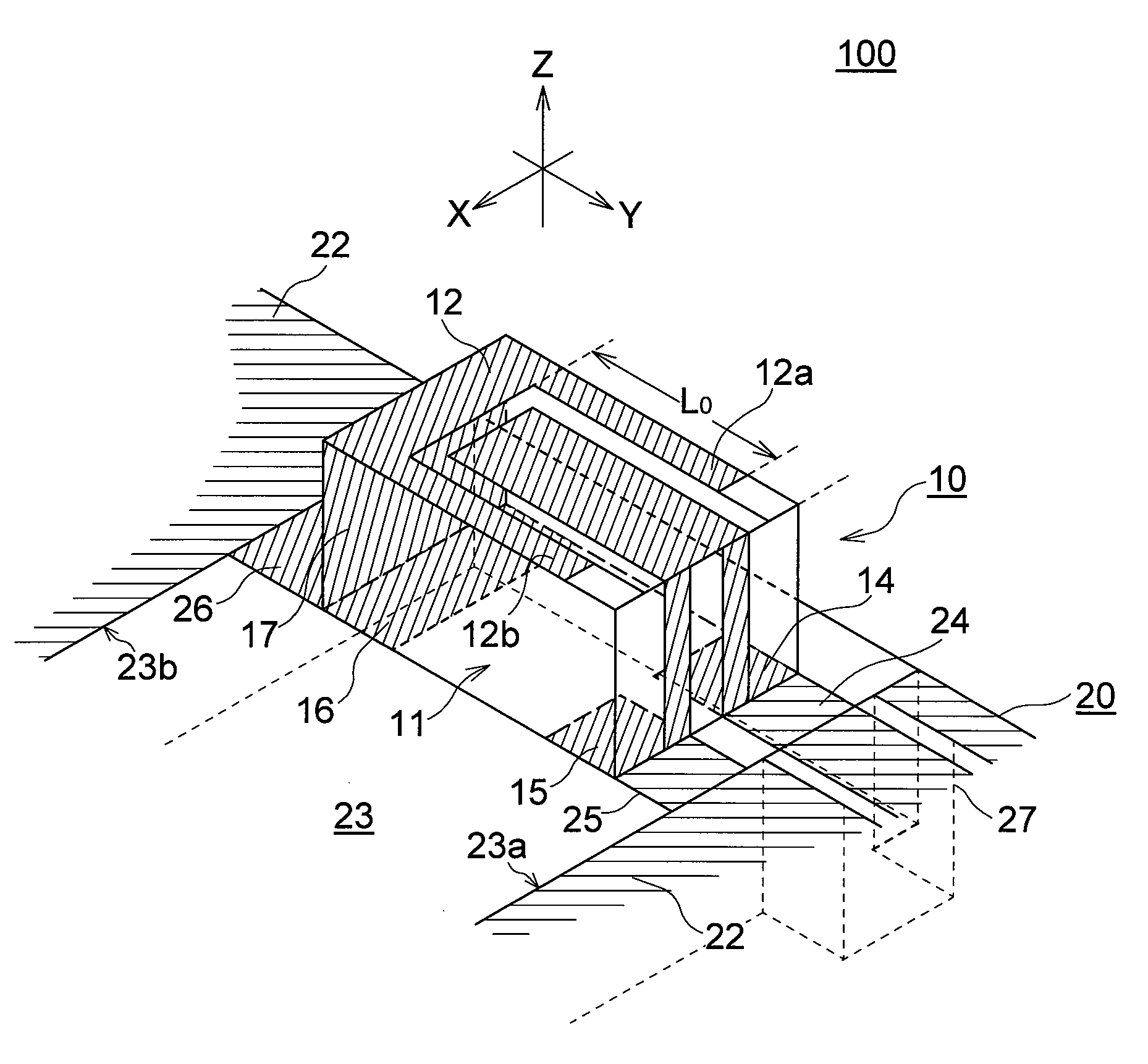
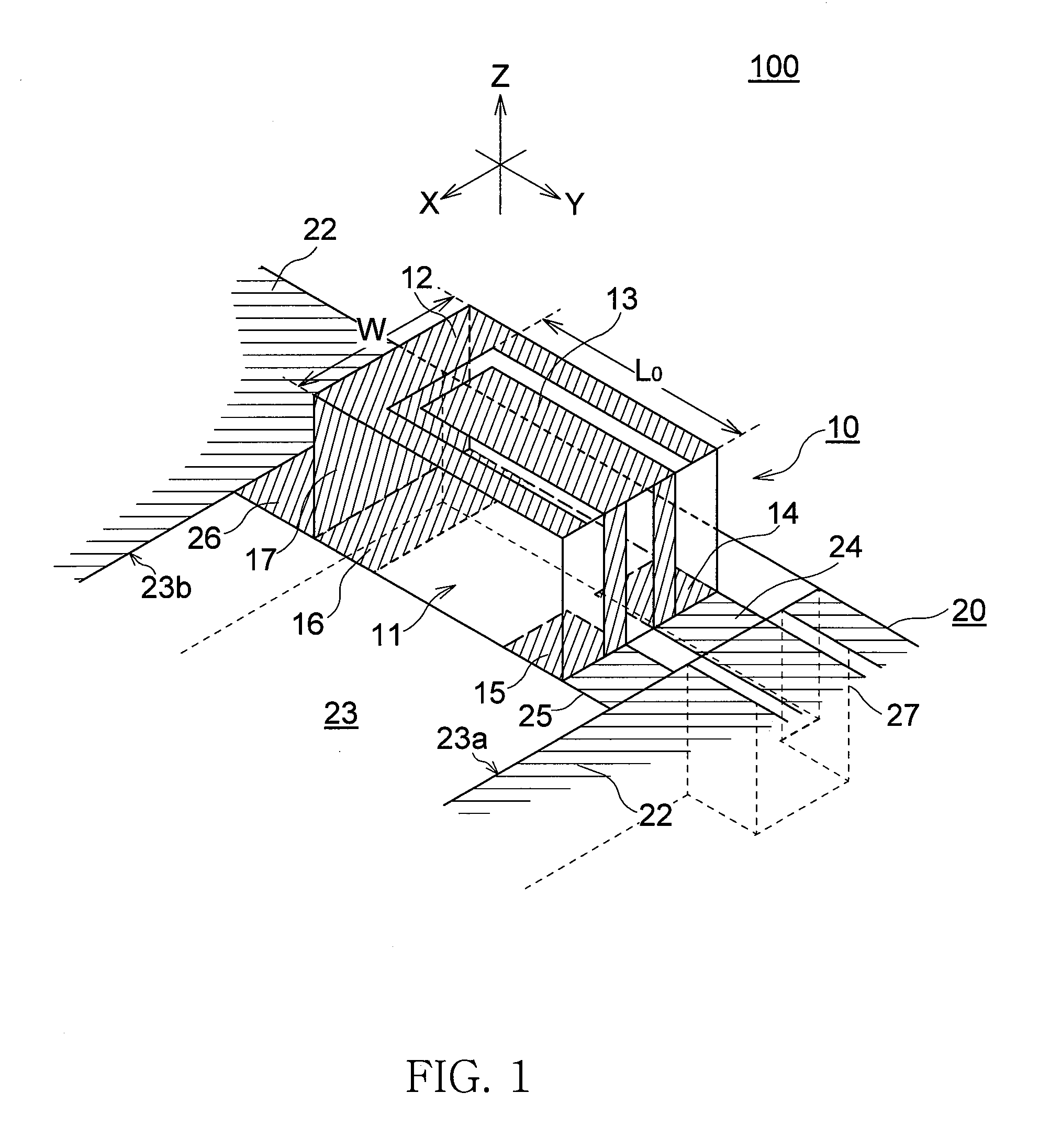
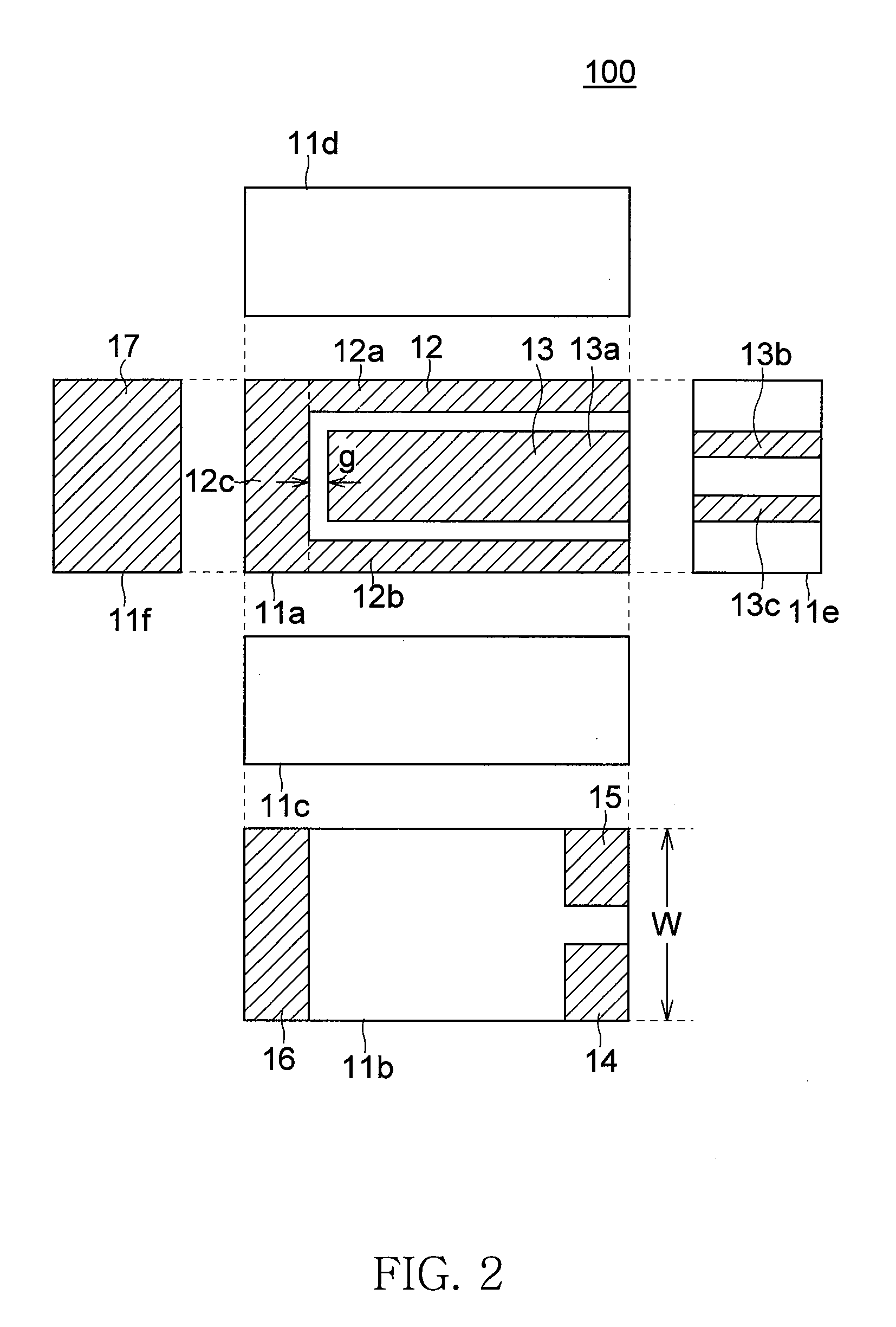
An antenna device is provided with an antenna element including a base, an inductance adjustment pattern that is formed on the upper surface and a side surface of the base and has a substantially U-shape, a capacitance adjustment pattern that is formed on the upper surface of the base and is placed to face the inductance adjustment pattern, and first to third terminal electrodes provided on the bottom surface of the base. The antenna element is installed between the first side and the second side of the ground pattern that form the two facing sides of the antenna mounting region. One end of the inductance adjustment pattern is connected to the feed line, the other end of the inductance adjustment pattern is connected to the first side of the ground pattern, and the third terminal electrode is connected to the second side of the ground pattern.

Description

TECHNICAL FIELD[0001]The present invention relates to an antenna device, and more particularly relates to a surface-mounted antenna device that is built in a small-size portable terminal such as a mobile-phone.BACKGROUND OF THE INVENTION[0002]In recent years, a chip antenna for GPS (Global Positioning System) or Bluetooth is built in a small-size portable terminal such as a mobile-phone. A chip antenna of this type is required to be small in size and to facilitate resonance frequency adjustment and impedance matching. This is because the resonance frequency and the input impedance of the chip antenna are affected by the structure of the printed circuit board, various electronic components mounted around the chip antenna, and the housing. Therefore, it is necessary to adjust the resonance frequency and the input impedance for each model.[0003]Particularly, it is very important to facilitate the input impedance adjustment of an antenna for the following reason. When the input impedanc...

Claims


Application Information

Patent Timeline
Patent Type & Authority Applications(United States)
IPC IPC(8): H01Q1/38H01Q1/50
CPCH01Q1/243H01Q9/42H01Q1/38
Inventor SHIMODA, HIDEAKISHIBATA, TETSUYASUZUKI, KEI
Owner TDK CORPARATION
Why Eureka
Try Eureka