Optical module

a technology of optical modules and optical elements, applied in the field of optical modules, can solve the problems of reducing the efficiency of optical coupling, the difficulty of manufacturing optical modules in this way, and the reduction of optical coupling efficiency, so as to achieve the effect of low risk of damaging optical elements or smearing the surface of optical elements

Inactive Publication Date: 2010-09-02
PANASONIC CORP
View PDF22 Cites 32 Cited by
  • Summary
  • Abstract
  • Description
  • Claims
  • Application Information

AI Technical Summary

Benefits of technology

[0008]It is an object of the present invention to provide an optical module which would not easily cause an optical axis offset between a polymer waveguide film and a submount, yet featuring high bond strength therebetween. It is another object of the invention to provide an optical module with low risk of damaging optical elements or smearing surfaces thereof in a bonding process. It is still another object of the invention to provide an optical module with low risk of a position offset between the polymer waveguide film and the submount and a resultant optical axis offset due to an inflow of adhesive.

Problems solved by technology

It is practically so difficult to manufacture optical modules that way.
Furthermore, even if the polymer waveguide film is manufactured with high dimensional accuracy and placed at a specified position on the submount, the polymer waveguide film might be displaced from the specified position when adhesive is filled into a gap between the polymer waveguide film and the submount, potentially causing an offset of optical axes of the polymer waveguide film and the submount and a resultant reduction in optical coupling efficiency.
This could potentially cause an optical axis offset between the polymer waveguide film and the submount and a resultant reduction in optical coupling efficiency.
Also, since the polymer waveguide film is positioned above optical elements, there is a risk of damaging the optical elements or smearing surfaces of the optical elements when placing the polymer waveguide film in position.
Furthermore, since the adhesive is filled into the gap between the polymer waveguide film in which the waveguide is provided and the submount carrying the optical elements, the distance between the waveguide and the optical elements might increase, potentially causing a reduction in optical coupling efficiency.

Method used


Image

  • Optical module
  • Optical module
  • Optical module

Examples


first embodiment

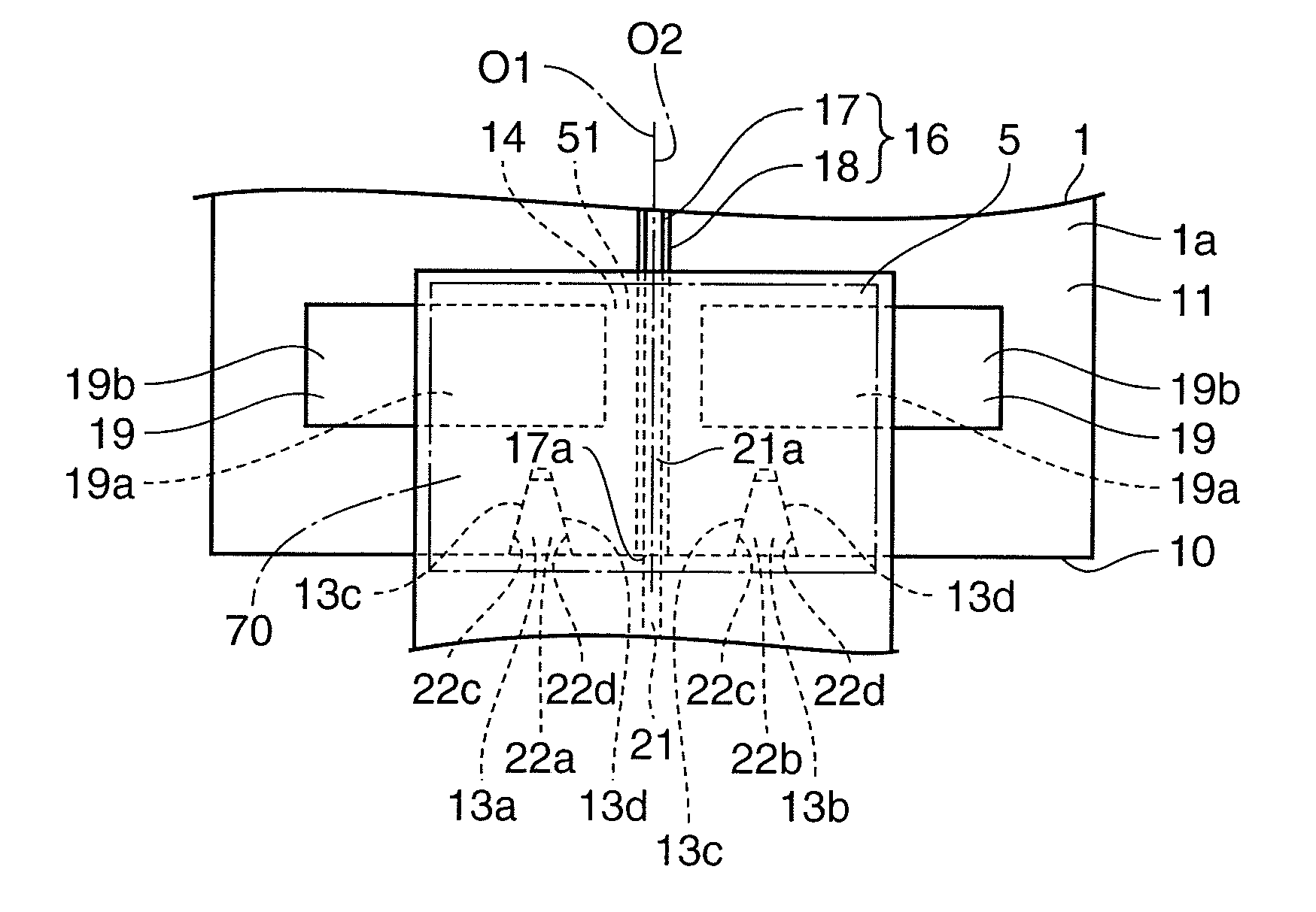
[0054]FIG. 1 is a schematic diagram of an optical module according to a first embodiment of the invention. As shown in FIG. 1, the optical module includes an emitter-side mounting substrate 1, a receiver-side mounting substrate 3 and an external waveguide substrate 2 which joins the two mounting substrates 1, 2 with optical coupling capability. As a convention in the following discussion of the present invention, “upward and downward directions” mean the upward and downward directions as illustrated in FIG. 1, “left and right directions” mean directions perpendicular to the plane of paper of FIG. 1, and left and right sides of FIG. 1 are regarded as front and rear of the optical module, respectively.

[0055]The emitter-side mounting substrate 1 has a generally rectangular shape in plan view which is elongate along a front-rear direction and has a thickness of approximately 200 μm to 2 mm. Overall dimensions of the mounting substrate 1 may differ depending on electrical and other compo...

second embodiment

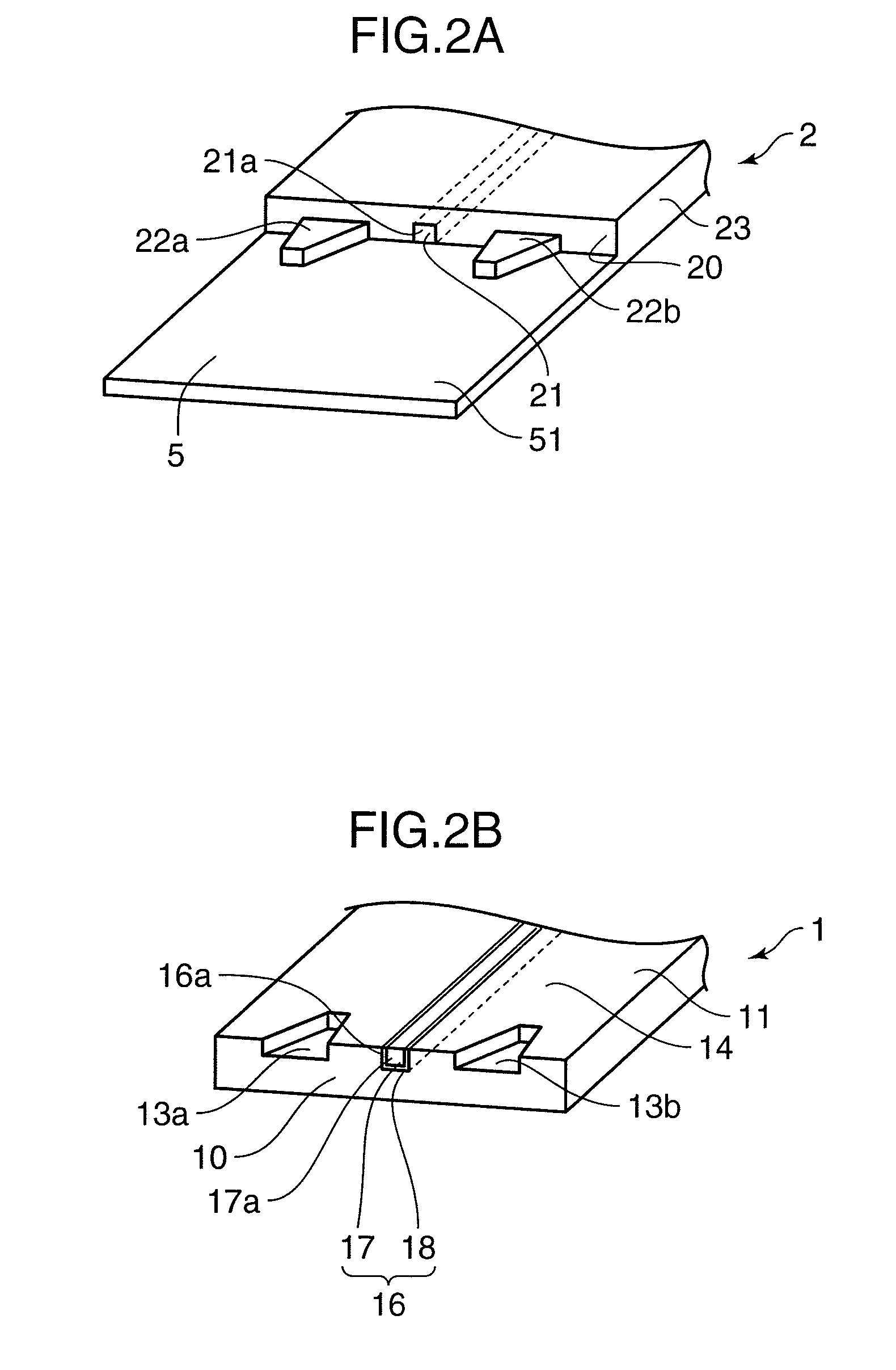
[0102]Now, an optical module according to a second embodiment of the invention is described with reference to FIGS. 6A and 6B. An emitter-side mounting substrate 100 of the optical module of the second embodiment has a single fitting recess 113.

[0103]Like the fitting recesses 13a, 13b formed in the mounting substrate 1 of the first embodiment, the fitting recess 113 has a left-side oblique wall 104 and a right-side oblique wall 105 which are formed such that the fitting recess 113 is generally dovetail-shaped (tapered) in plan view, gradually narrowing frontward as depicted in FIG. 6B. In this embodiment, the left-side oblique wall 104 is located on a left side of an axis O1 of a core 17 of a waveguide 16 and the right-side oblique wall 105 is located on a right side of the axis O1 of the core 17 of the waveguide 16. Also, the left- and right-side oblique walls 104, 105 are formed symmetrically on the left and right sides of the axis O1 of the core 17 of the waveguide 16, respective...

third embodiment

[0106]Next, an optical module according to a third embodiment of the invention is described. An emitter-side mounting substrate 301 of the optical module of this embodiment has a plurality of adhesive filling recesses 319 which are formed close to left and right rear portions of each of fitting recesses 313a, 313b in such a manner that the adhesive filling recesses 319 connect to the respective fitting recesses 313a, 313b.

[0107]Referring to FIG. 7B, a lap joint portion 305 of an external waveguide substrate 2 has a pair of fitting tabs 322a, 322b, each of the fitting tabs 322a, 322b having a left-side contact wall 322c and a right-side contact wall 322d. Basal parts of the left- and right-side contact walls 322c, 322d serve as bonding areas 320.

[0108]After the plurality of adhesive filling recesses 319 have been filled with the adhesive, the fitting tabs 322a, 322b of the lap joint portion 305 of the external waveguide substrate 2 are fitted into the fitting recesses 313a, 313b of ...


PUM


Abstract

An optical module includes an emitter-side mounting substrate, a receiver-side mounting substrate and an external waveguide substrate. The mounting substrate is provided with a waveguide having a core and a pair of fitting recesses. The external waveguide substrate is provided with an external waveguide having a core, a pair of fitting tabs and a lap joint portion. As the fitting tabs are fitted into the respective fitting recesses, the mounting substrate and the external waveguide substrate are joined together, the two cores are aligned with each other, and the lap joint portion is positioned to overlap the mounting substrate.

Description

TECHNICAL FIELD[0001]The present invention relates to an optical module configured to transmit or receive an optical signal.BACKGROUND ART[0002]A conventionally known optical module used for transmission or reception of an optical signal is configured such that a polymer waveguide film (external waveguide substrate) having a waveguide (optical waveguide) with a core formed therein is bonded to a submount (referred to as a mounting substrate in this invention) carrying one or more optical elements (e.g., a light-emitting element and / or a light-detecting element) by adhesive with the polymer waveguide film positioned above the optical element(s) of the submount, whereby light emitted from the optical element is coupled to an incident end surface of the waveguide (refer to Patent Document 1).[0003]Patent Document 1: Japanese Laid-open Patent Application No. 2006-243467[0004]If, however, the polymer waveguide film is to be bonded to the submount in the aforementioned fashion, it is esse...

Claims


Application Information

Patent Timeline
Patent Type & Authority Applications(United States)
IPC IPC(8): G02B6/42
CPCG02B6/423G02B6/43G02B6/4239G02B6/12G02B6/26G02B6/42
Inventor ASAHI, NOBUYUKINISIMURA, MAKOTOMIYAGAWA, NOBUYUKIYAGYU, HIROYUKIUCHIDA, YUICHIKINUGASA, YUTAKAYAMAJI, TADAHIROMATSUMOTO, TAKUYA
Owner PANASONIC CORP
Why Eureka
Try Eureka