Charged particle beam writing apparatus and optical axis deviation correcting method for charged particle beam

a writing apparatus and charge technology, applied in the field of charged particle beam writing apparatus and optical axis deviation correcting method for charged particle beam, can solve the problems of deteriorating pattern dimensional accuracy, on-axis astigmatism, and deflection distortion

Active Publication Date: 2010-09-09
NUFLARE TECH INC
View PDF3 Cites 6 Cited by
  • Summary
  • Abstract
  • Description
  • Claims
  • Application Information

AI Technical Summary

Benefits of technology

[0012]It is an object of the present invention to provide a method and apparatus which corrects a deviation of an optical axis of a beam even though the beam is turned ON / OFF at a high speed.

Problems solved by technology

When a high-frequency pulse serving as a blanking signal to control ON / OFF state of an electron beam is applied across electrodes of the blanker having the above configuration by using the writing apparatus having the optical axis adjusted as described above, the optical axis of the electron beam which should have been adjusted may be disadvantageously deviated.
The decrease in dose of the electron beam causes a problem such as deterioration of pattern dimensional accuracy.
Furthermore, when the optical axis of the electron beam is deviated, the electron beam does not pass through the center of an electron lens such as an objective lens through which the electron beam were to pass thereafter to also cause an on-axis astigmatism, a deflection astigmatism, and a deflection distortion.
As described above, when a high-frequency pulse is applied across the electrodes of the blanker having the above configuration, the optical axis of the electron beam which should have been adjusted is disadvantageously deviated.
As described above, when the optical axis of the electron beam is deviated, a problem such as deterioration in pattern dimensional accuracy, an on-axis astigmatism, a deflection astigmatism, or a deflection distortion may be caused.
However, conventionally, a method of solving the problem has not been established yet.

Method used


Image

  • Charged particle beam writing apparatus and optical axis deviation correcting method for charged particle beam
  • Charged particle beam writing apparatus and optical axis deviation correcting method for charged particle beam
  • Charged particle beam writing apparatus and optical axis deviation correcting method for charged particle beam

Examples


embodiment 1

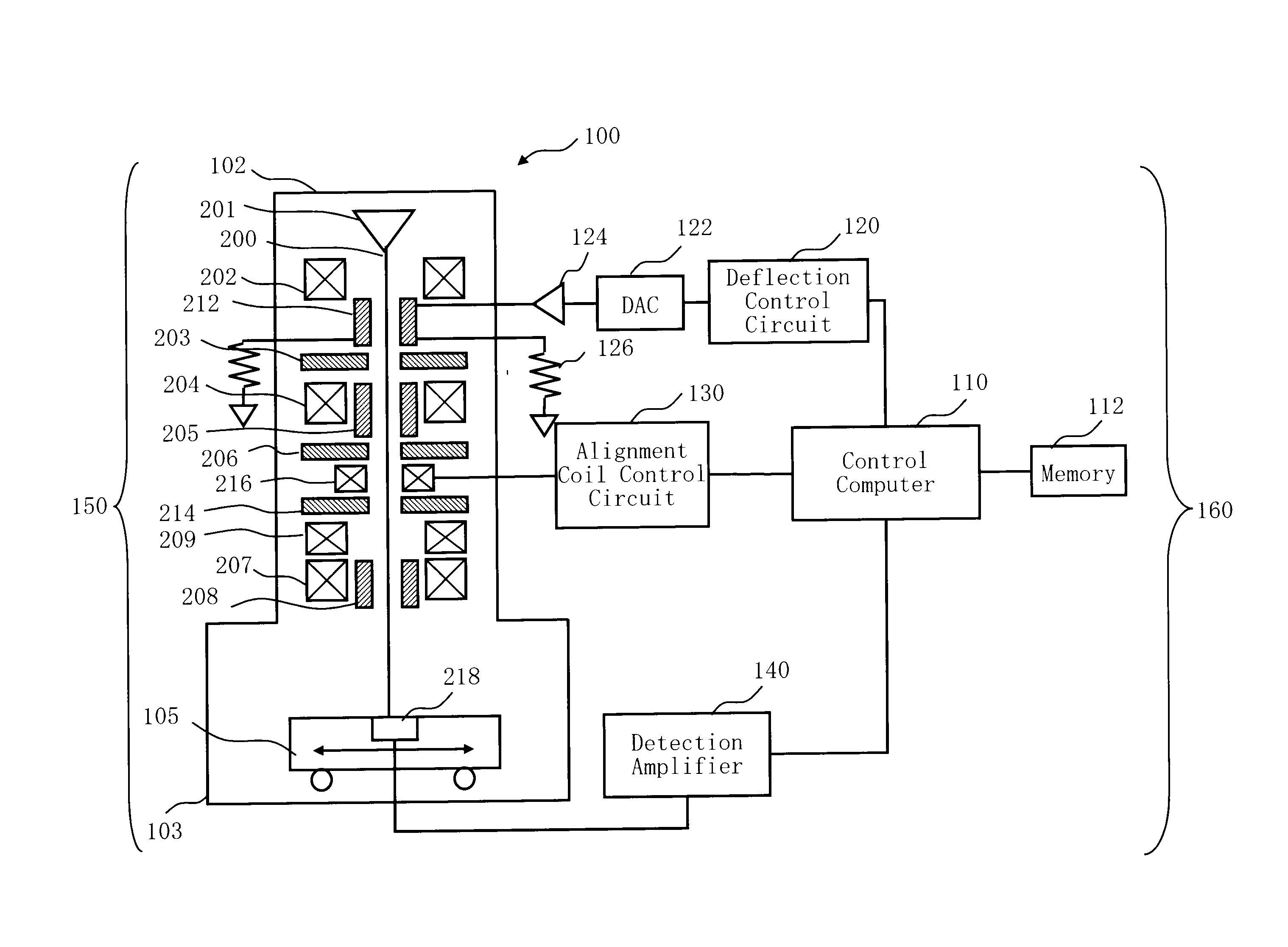
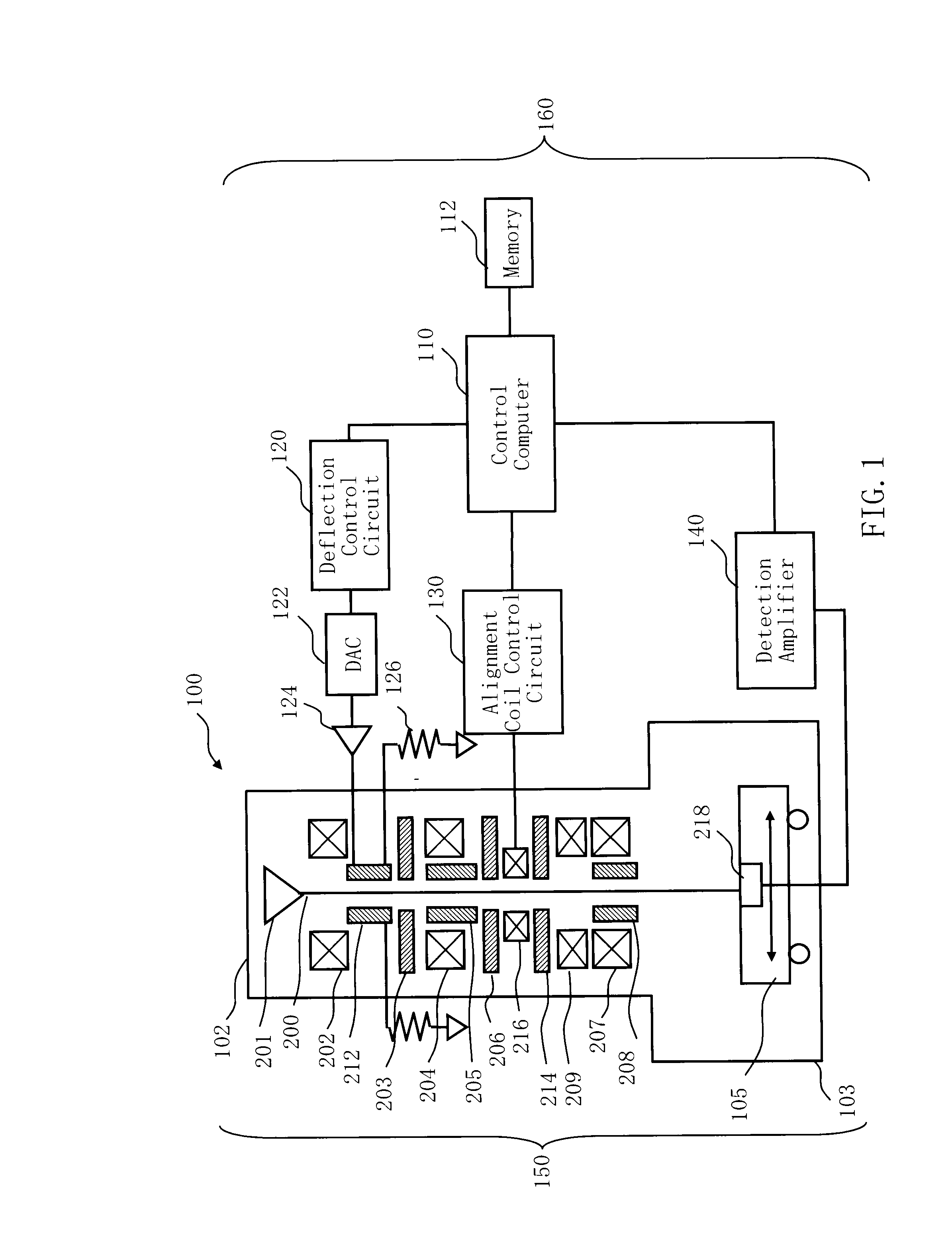
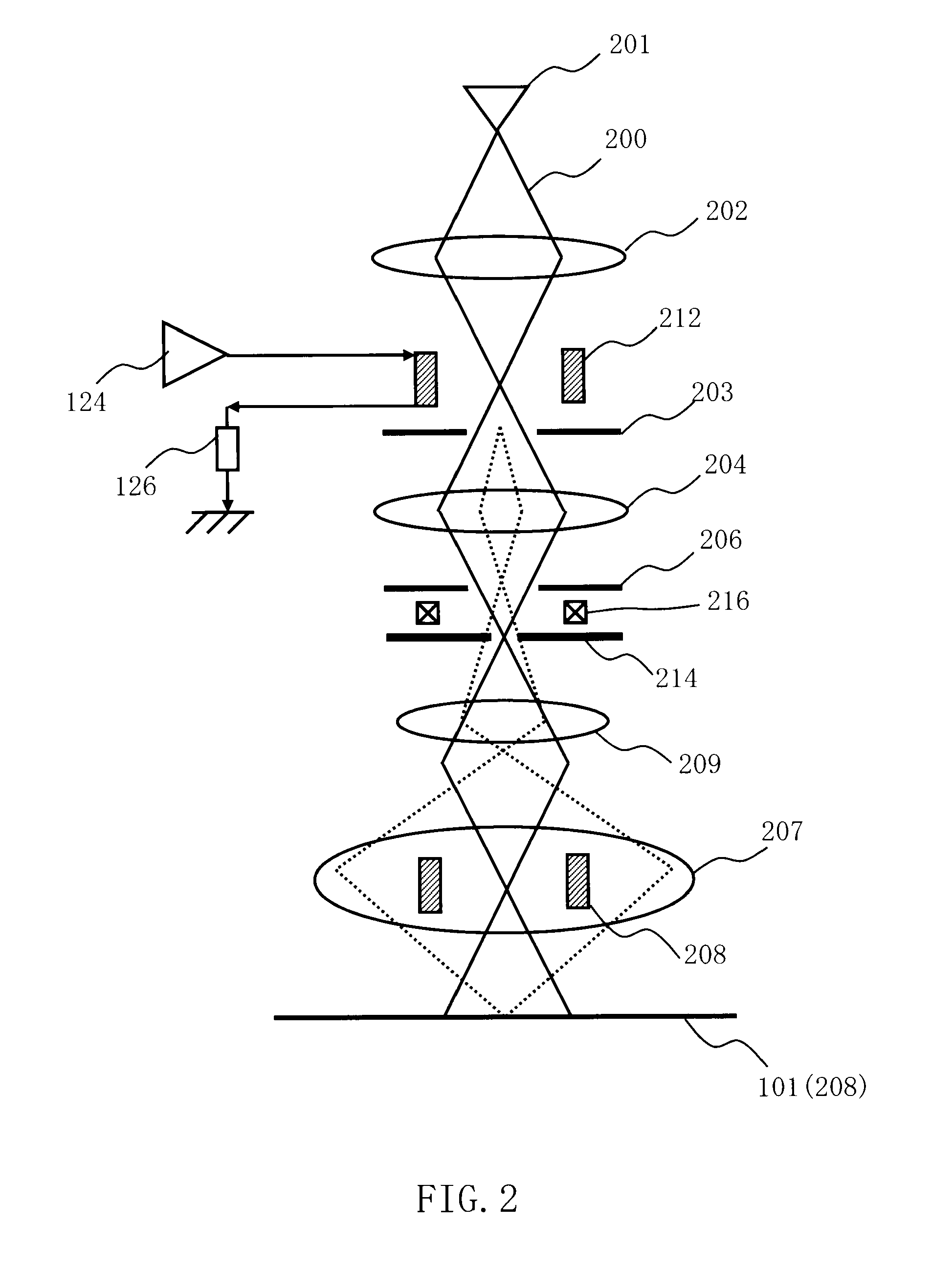
[0023]In an embodiment, a configuration using an electron beam as an example of a charged particle beam will be described below. The charged particle beam is not limited to an electron beam, and a beam such as an ion beam using charged particles may be used.

[0024]FIGS. 1 and 2 are conceptual diagrams showing a configuration of an electron beam writing apparatus according to Embodiment 1. In FIGS. 1 and 2, a writing apparatus 100 includes a write unit 150 and a control unit 160. The writing apparatus 100 serves as an example of a charged particle beam writing apparatus. The write unit 150 has an electron lens barrel 102 and a write chamber 103. In the electron lens barrel 102, an electron gun assembly 201 (emitting unit), an illumination lens 202, a blanker 212, a first aperture plate 203, a projection lens 204, a deflector 205, a second aperture plate 206, an alignment coil 216, a blanking aperture plate 214 (regulation aperture plate), a reducing lens 209, an objective lens 207, an...


PUM


Abstract

A charged particle beam writing apparatus includes a stage on which a target object is placed; an emitting unit configured to emit a charged particle beam to the stage side; a blocking unit arranged between the emitting unit and the stage and configured to block the charged particle beam emitted; a deflector having electrodes through which a current flows by applying a voltage and configured to deflect the charged particle beam passing between the electrodes onto the blocking unit by applying a predetermined voltage across the electrodes; an optical axis adjusting unit configured to correct optical axis deviation of the charged particle beam generated by continuously repeating irradiation (beam-ON) of the charged particle beam on a target object and blocking (beam-OFF) of the beam by applying a two-step voltage to the deflector; and a control unit configured to control the optical axis adjusting unit such that an amount of the optical axis deviation is corrected.

Description

CROSS-REFERENCE TO RELATED APPLICATION[0001]This application is based upon and claims the benefit of priority from prior Japanese Patent Application No. 2009-052995 filed on Mar. 6, 2009 in Japan, the entire contents of which are incorporated herein by reference.BACKGROUND OF THE INVENTION[0002]1. Field of the Invention[0003]The present invention relates to a charged particle beam writing apparatus and an optical axis deviation correcting method for a charged particle beam, for example, correction for optical axis deviation of an electron beam in a writing apparatus which forms a pattern on a target object while variably shaping the electron beam.[0004]2. Related Art[0005]A lithography technique which takes a part of the development of miniaturization of semiconductor devices is only a process, in which a pattern is generated, in semiconductor manufacturing processes and is very important. In recent years, with the advancement in integration density of an LSI, circuit line widths re...

Claims


Application Information

Patent Timeline
Patent Type & Authority Applications(United States)
IPC IPC(8): H01J37/30H01J37/147H01J3/26
CPCB82Y10/00B82Y40/00H01J37/1471H01J37/1474H01J2237/24405H01J37/317H01J37/3174H01J2237/1501H01J37/3045
Inventor SAKAI, MICHIHIROKAKEHI, RYOICHIHATTORI, KIYOSHI
Owner NUFLARE TECH INC
Why Eureka
Try Eureka