Integrated Semiconductor Structure with a Solar Cell and a Bypass Diode

a solar cell and integrated semiconductor technology, applied in the direction of semiconductor devices, sustainable manufacturing/processing, climate sustainability, etc., can solve the problems of degrading the cell, cell inoperable, and the inability of solar cells to meet the needs of more sophisticated applications, so as to achieve the effect of maximizing the energy efficiency of solar cells

Inactive Publication Date: 2010-09-23
SOLAERO TECH CORP
View PDF5 Cites 45 Cited by
  • Summary
  • Abstract
  • Description
  • Claims
  • Application Information

AI Technical Summary

Benefits of technology

[0018]It is another object of the invention to provide an integral bypass diode in a multi-solar cell structure, with at least two adjacent lattice mismatched subcells that maximizes the energy efficiency of the solar cell.

Problems solved by technology

While significant progress has been made in this area, the requirement for solar cells to meet the needs of more sophisticated applications has not kept pace with demand.
However, if any of the cells are not illuminated, because of shadowing or damage, those shadowed cells are still in the array circuit and may be forced to become reversed biased in order to carry the current generated by the illuminated cells.
This reverse biasing can degrade the cells and can ultimately render the cells inoperable.
However, when the solar cell is not receiving sunlight, whether because of shading by a movement of the satellite, or as a result of damage to the cell, then resistance exists along the cell path.
If there were no diode, the current would force its way through the cell layers, reversing the bias of such cells and permanently degrading, if not destroying the electrical characteristics of such cells.
The problem with this concept has been the difficulty in creating a diode that is relatively easy to manufacture and which uses a very low level of voltage to turn on and operate.
However, in a multijunction solar cell with a germanium substrate, to pass through the Ge junction the bias of the Ge junction must be reversed, requiring a large voltage.

Method used


Image

  • Integrated Semiconductor Structure with a Solar Cell and a Bypass Diode
  • Integrated Semiconductor Structure with a Solar Cell and a Bypass Diode
  • Integrated Semiconductor Structure with a Solar Cell and a Bypass Diode

Examples


Embodiment Construction

[0039]Details of the present invention will now be described including exemplary aspects and embodiments thereof. Referring to the drawings and the following description, like reference numbers are used to identify like or functionally similar elements, and are intended to illustrate major features of exemplary embodiments in a highly simplified diagrammatic manner. Moreover, the drawings are not intended to depict every feature of the actual embodiment nor the relative dimensions of the depicted elements, and are not drawn to scale.

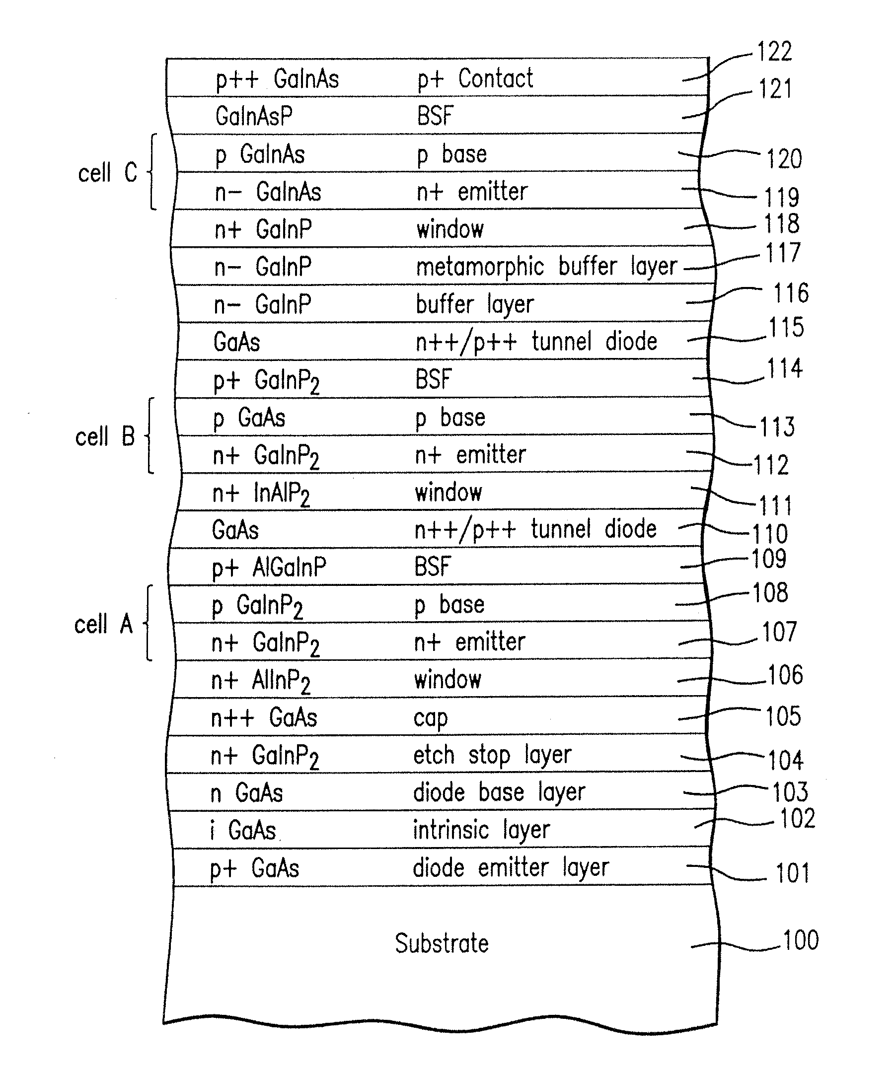
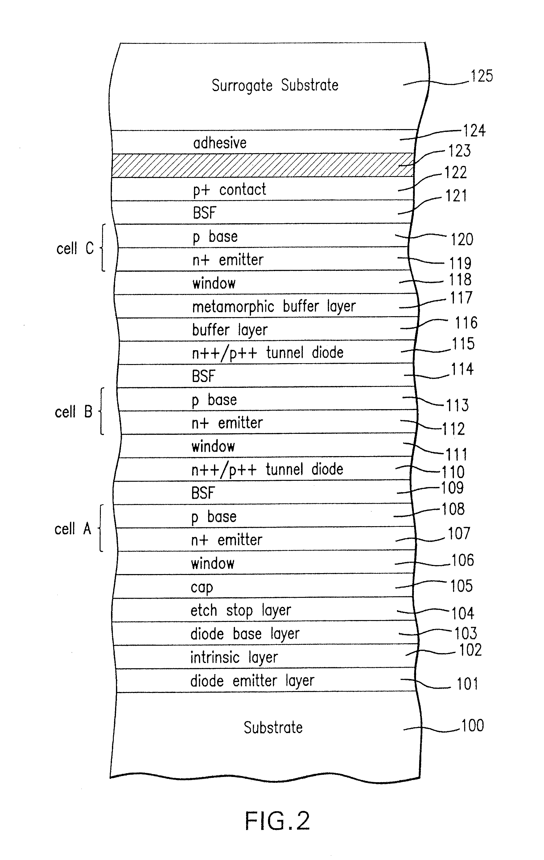
[0040]FIG. 1 depicts the multijunction solar cell according to the present invention after formation of the three subcells A, B and C on a substrate. More particularly, there is shown a substrate 100, which may be either gallium arsenide (GaAs), germanium (Ge), or other suitable material. A sequence of layers forming a diode is then deposited on the substrate. For example, a p+ GaAs diode emitter layer 101, an intrinsic GaAs layer 102, and a n type GaAs ...


PUM


Abstract

An integral semiconductor device having a sequence of layers of semiconductor material. The semiconductor device may include a first region in which the sequence of layers of semiconductor material forms at least one cell of a multijunction solar cell including a metamorphic layer with a graded lattice constant. The semiconductor device may also include a second region, spaced apart from the first region, in which the sequence of layers in the second region forms a support for a bypass diode that functions to pass current when the solar cell is shaded.

Description

REFERENCE TO RELATED APPLICATIONS[0001]This application is a division of U.S. patent application Ser. No. 11 / 614,332, filed Dec. 21, 2006. This application also is related to co-pending U.S. patent application Ser. No. 11 / 445,793 filed Jun. 2, 2006.BACKGROUND OF THE INVENTION[0002]1. Field of the Invention[0003]The present invention relates to the field of solar cell semiconductor devices, and particularly to integrated semiconductor structures including a multijunction solar cell and an integral bypass diode.[0004]2. Description of the Related Art[0005]Photovoltaic cells, also called solar cells, are one of the most important new energy sources that have become available in the past several years. Considerable effort has gone into solar cell development. As a result, solar cells are currently being used in a number of commercial and consumer-oriented applications. While significant progress has been made in this area, the requirement for solar cells to meet the needs of more sophis...

Claims


Application Information

Patent Timeline
Patent Type & Authority Applications(United States)
IPC IPC(8): H01L31/102H01L31/078
CPCY02E10/544H01L27/1421H01L31/06875H01L31/0443Y02E10/547Y02P70/50
Inventor SHARPS, PAUL R.
Owner SOLAERO TECH CORP
Why Eureka
Try Eureka