Selectively self-assembling oxygen diffusion barrier

a diffusion barrier and self-assembling technology, applied in the field of semiconductor structure, can solve the problems of limiting the performance of conventional semiconductor oxide based gate electrodes, increasing processing complexity and cost, and degrading the device characteristics of semiconductor devices formed on the semiconductor surfa

Active Publication Date: 2010-09-23
GLOBALFOUNDRIES US INC
View PDF2 Cites 62 Cited by
  • Summary
  • Abstract
  • Description
  • Claims
  • Application Information

AI Technical Summary

Benefits of technology

[0007]The present invention provides a selectively self-assembling oxygen barrier layer formed between an oxide-containing structure such as a shallow trench isolation structure in a semiconductor substrate and a high dielectric constant (high-k) material structure such as a gate dielectric, and methods of manufacturing the same.

Problems solved by technology

High gate leakage current of silicon oxide and nitrided silicon dioxide as well as depletion effect of polysilicon gate electrodes limits the performance of conventional semiconductor oxide based gate electrodes.
Formation of an oxygen barrier layer only on the top surface of shallow trench isolation structures by deposition and lithographic patterning increases processing complexity and cost.
Nitridation of shallow trench isolation structures invariably induces nitridation of exposed semiconductor surfaces, which degrades device characteristics of semiconductor devices formed on the semiconductor surfaces.

Method used


Image

  • Selectively self-assembling oxygen diffusion barrier
  • Selectively self-assembling oxygen diffusion barrier
  • Selectively self-assembling oxygen diffusion barrier

Examples


Embodiment Construction

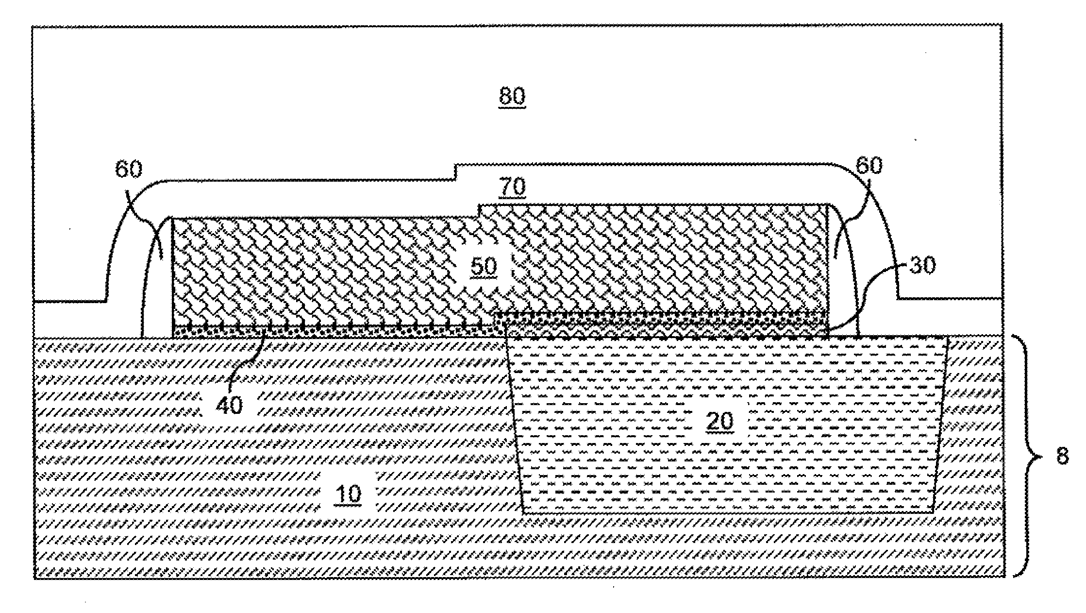
[0016]As stated above, the present invention relates to a semiconductor structure including a selectively self-assembling oxygen diffusion barrier located between an oxide-containing structure in a semiconductor substrate and a high dielectric constant (high-k) material structure and methods of manufacturing the same, which are now described in detail with accompanying figures. Like and corresponding elements are referred to by like reference numerals.

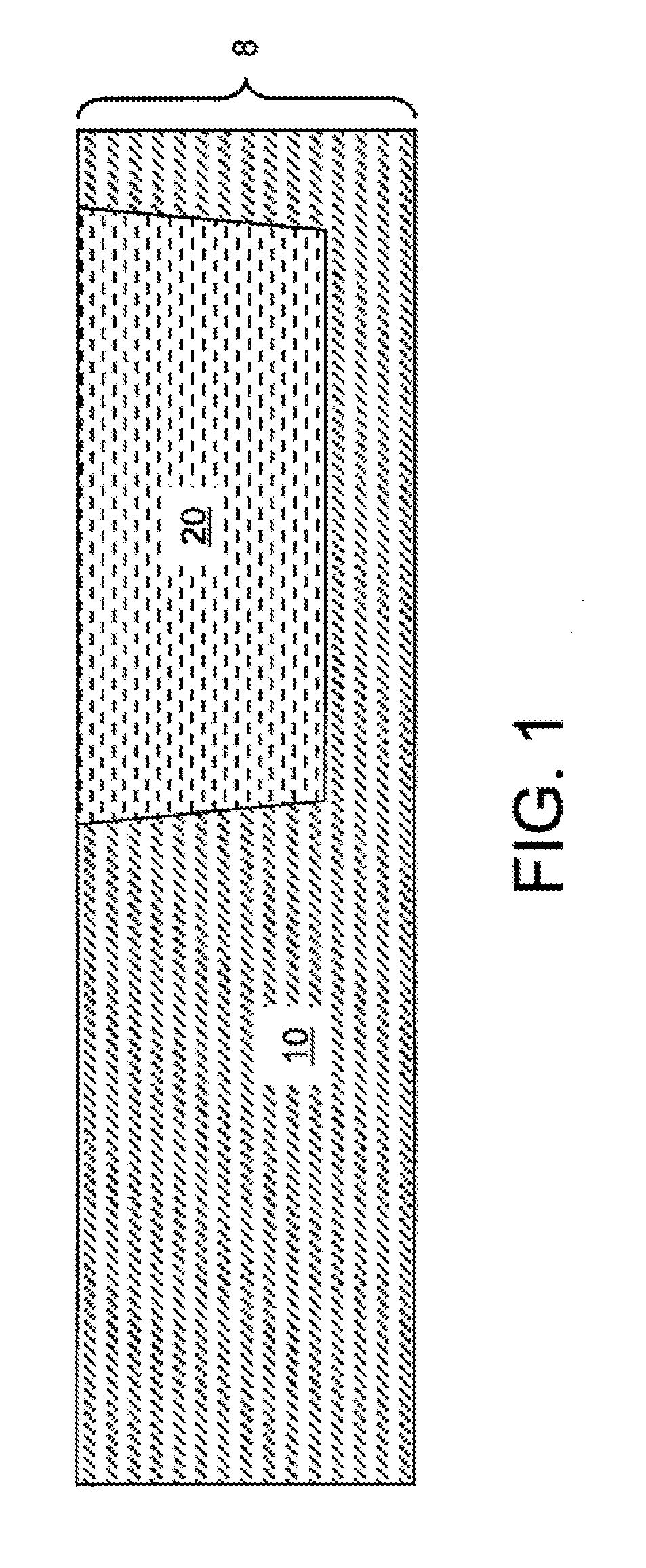
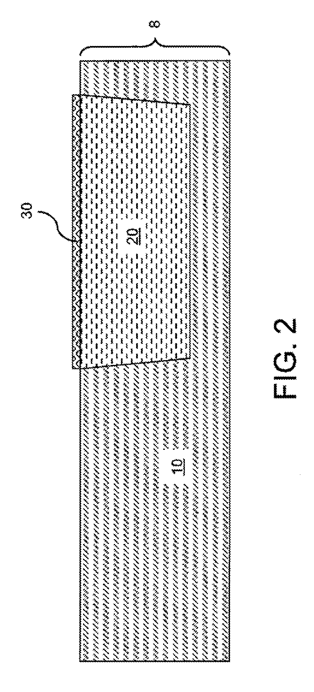
[0017]Referring to FIG. 1, an exemplary semiconductor structure according to the present invention is shown, which comprises a substrate 8 including a semiconductor material portion 10 and a dielectric material portion 20. The dielectric material portion 20, which is embedded in the semiconductor material portion 10, has an exposed upper surface. For example, the dielectric material portion 20 may be a shallow trench isolation (STI) structure that laterally surrounds an active region of the semiconductor material portion 10 on which a ...


PUM


Abstract

A shallow trench isolation structure is formed in a semiconductor substrate adjacent to an active semiconductor region. A selective self-assembling oxygen barrier layer is formed on the surface of the shallow trench isolation structure that includes a dielectric oxide material. The formation of the selective self-assembling oxygen barrier layer is selective in that it is not formed on the surface the active semiconductor region having a semiconductor surface. The selective self-assembling oxygen barrier layer is a self-assembled monomer layer of a chemical which is a derivative of alkylsilanes including at least one alkylene moiety. The silicon containing portion of the chemical forms polysiloxane, which is bonded to surface silanol groups via Si—O—Si bonds. The monolayer of the chemical is the selective self-assembling oxygen barrier layer that prevents diffusion of oxygen to a high dielectric constant material layer that is subsequently deposited as a gate dielectric.

Description

FIELD OF THE INVENTION[0001]The present invention relates to a semiconductor structure including a selectively self-assembling oxygen diffusion barrier located between an oxide-containing structure in a semiconductor substrate and a high dielectric constant (high-k) material structure, and methods of manufacturing the same.BACKGROUND OF THE INVENTION[0002]High gate leakage current of silicon oxide and nitrided silicon dioxide as well as depletion effect of polysilicon gate electrodes limits the performance of conventional semiconductor oxide based gate electrodes. High performance devices for an equivalent oxide thickness (EOT) less than 1 nm require high dielectric constant (high-k) gate dielectrics and metal gate electrodes to limit the gate leakage current and provide high on-currents. High dielectric constant typically refers to a dielectric constant grater than 4.0. Materials for high-k gate dielectrics include ZrO2, HfO2, other dielectric metal oxides, alloys thereof, and thei...

Claims


Application Information

Patent Timeline
Patent Type & Authority Applications(United States)
IPC IPC(8): H01L29/78H01L21/31
CPCH01L21/02126H01L21/02211H01L21/02282H01L21/28123H01L21/3105H01L29/518H01L21/76224H01L29/495H01L29/4966H01L29/517H01L21/3121
Inventor LI, ZHENGWENROTONDARO, ANTONIO L.P.VISOKAY, MARK R.
Owner GLOBALFOUNDRIES US INC
Why Eureka
Try Eureka