Semiconductor device and method of manufacturing the same, and electronic apparatus

a semiconductor and semiconductor technology, applied in the field of semiconductor devices, can solve the problems of limited connection conductor materials, increased cost, and difficulty in practicability, and achieve the effects of high-performance semiconductor devices, excellent mass productivity and cost effectiveness, and sufficient performance capabilities

Active Publication Date: 2010-09-23
SONY CORP
View PDF13 Cites 203 Cited by
  • Summary
  • Abstract
  • Description
  • Claims
  • Application Information

AI Technical Summary

Benefits of technology

[0029]In the semiconductor device according to any of the embodiments of the present invention, the pixel array and the logic circuit that exert their respective sufficient performance capabilities are formed in each microchip part. Thus, a high-performance semiconductor device, or a back-illuminated solid-state imaging device, can be provided. In addition, the high-performance back-illuminated solid-state imaging device with excellent mass productivity and cost effectiveness can be provided.
[0030]In the semiconductor device according to any of the embodiments of the present invention, furthermore, the first semiconductor integrated circuit and the second semiconductor integrated circuit that exert their respective sufficient performance capabilities are formed in each microchip part. Therefore, a high-performance semiconductor device can be provided. In addition, the high-performance semiconductor device with excellent mass productivity and cost effectiveness can be provided.
[0031]In the method of manufacturing the semiconductor device according to any of the embodiments of the present invention, under the optimal proce

Problems solved by technology

Thus, it is practically difficult from the viewpoints of the processing of a connection hole and the cost effectiveness of a process for embedding a connection conductor.
In this case, however, some complicated steps, such as one for bonding the upper chip on a supporting substrate, may be de

Method used


Image

  • Semiconductor device and method of manufacturing the same, and electronic apparatus
  • Semiconductor device and method of manufacturing the same, and electronic apparatus
  • Semiconductor device and method of manufacturing the same, and electronic apparatus

Examples


first embodiment

2. First Embodiment

Example of Configuration of Solid-State Imaging Device and Example of Method of Manufacturing the Solid-State Imaging Device

[0081]Referring now to FIG. 3 and FIGS. 4 to 13, a semiconductor device (i.e., a MOS solid-state imaging device) and a method of manufacturing the solid-state imaging device will be described.

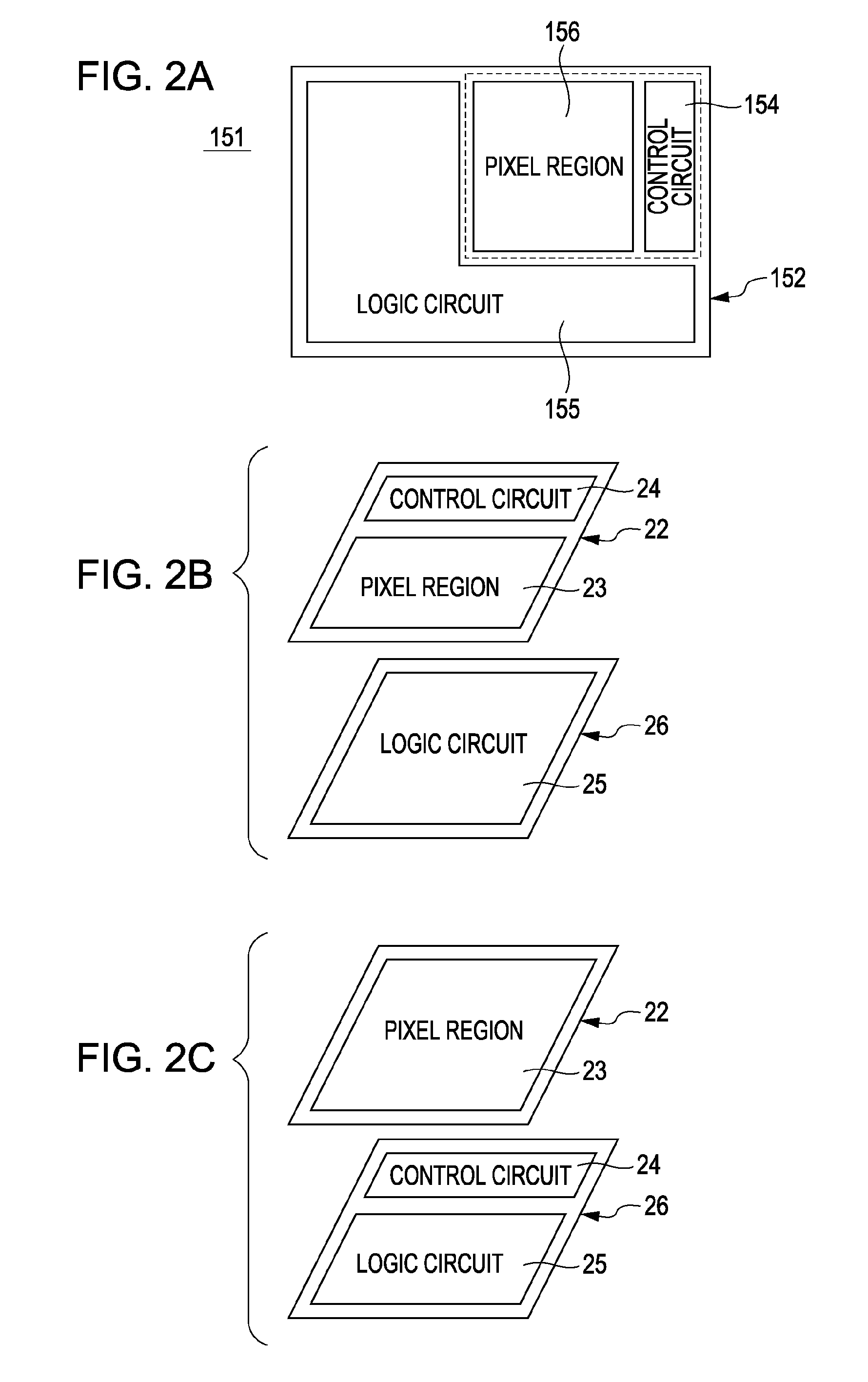
[0082]In the first embodiment, first, as shown in FIG. 4, a half-finished image sensor, or an pixel array (hereinafter, also referred to as a pixel region) 23, and a control circuit (control region) 24 are formed on a region to be provided as each microchip part of a first semiconductor wafer (hereinafter, also referred to as a semiconductor substrate) 31. In other words, a photodiode (PD), which acts as a photoelectric conversion part of each pixel, is formed on a region to be formed as each microchip part of the semiconductor substrate (for example, a silicon substrate) 31. Then, a source / drain region 33 of each pixel transistor is formed on a semicond...

second embodiment

3. Second Embodiment

Example of Configuration of Solid-State Imaging Device

[0108]Referring now to FIG. 14, a solid-state imaging device (i.e., a MOS solid-state imaging device) according to a second embodiment of the present invention will be described. The solid-state imaging device 81 according to the second embodiment of the present invention is constructed in a manner similar to that of the first embodiment, except for the followings: In this embodiment, only the electrode pad 72 on the side of the first semiconductor substrate 31 is formed, while the connection conductor 51, the insulating layer 52, and the electrode bump 78 on the side of the second semiconductor substrate 45 are omitted. In addition, a passivation layer 76 is formed on the back side of the second semiconductor substrate 45. Other structural components are the same as those described in the first embodiment. Therefore, the corresponding structural components are designated by the same reference numerals as thos...

third embodiment

4. Third Embodiment

Example of Configuration of Solid-State Imaging Device

[0110]Referring now to FIG. 15, a semiconductor device (i.e., a MOS solid-state imaging device) according to a third embodiment of the present invention will be described. In the solid-state imaging device 83 of the third embodiment, the pixel region 23 and the control circuit 24 formed on the side of the first semiconductor substrate 31 are electrically connected to the logic circuit 25 on the side of the second semiconductor substrate 45 through one through-connection conductor 84 formed in the first semiconductor substrate 31.

[0111]In other words, a connection through-hole 85 is formed such that it extends from the back side 31b of the first semiconductor substrate to the uppermost layer of the wiring 53 of the second semiconductor substrate 45 through the first semiconductor substrate 31. In addition, part of the connection through-hole 85 reaches to the uppermost layer of the wiring 40 of the first semicon...


PUM


Abstract

A semiconductor device is provided as a back-illuminated solid-state imaging device. The device is manufactured by bonding a first semiconductor wafer with a pixel array in a half-finished product state and a second semiconductor wafer with a logic circuit in a half-finished product state together, making the first semiconductor wafer into a thin film, electrically connecting the pixel array and the logic circuit, making the pixel array and the logic circuit into a finished product state, and dividing the first semiconductor wafer and the second semiconductor being bonded together into microchips.

Description

BACKGROUND OF THE INVENTION[0001]1. Field of the Invention[0002]The present invention relates to a semiconductor device, such as a solid-state imaging device, and a method of manufacturing such a semiconductor device. The present invention also relates to an electronic apparatus, such as a camera, equipped with the semiconductor device.[0003]2. Description of the Related Art[0004]Solid-state imaging devices, which have been commonly used, include amplification-type solid-state imaging devices as typified by MOS image sensors such as complementary metal oxide semiconductors (CMOSs) and charge-transfer solid-state imaging devices as typified by charge coupled device (CCD) image sensors. These solid-state imaging devices have been widely used for digital still cameras, digital video cameras, and so on. Furthermore, in recent years, MOS image sensors have been used for most of solid-state imaging devices mounted on mobile devices such as camera cell-phones and PDAs (Personal Digital Ass...

Claims


Application Information

Patent Timeline
IPC IPC(8): H04N5/335H01L31/14H01L31/18H01L27/146H01L21/02H01L27/00H01L27/14H04N5/369H04N5/374
CPCH01L27/14632H01L27/1469H01L27/14645H01L27/14636H01L27/1464H01L27/14687H01L27/14634H01L2224/11H01L21/76898H01L23/481H01L27/14621H01L27/14627H01L27/14612H01L27/14643H04N25/79H04N23/00H04N25/76
Inventor UMEBAYASHI, TAKUTAKAHASHI, HIROSHISHOHJI, REIJIROH
Owner SONY CORP
Why Eureka
Try Eureka