Substrate etching method and system
- Summary
- Abstract
- Description
- Claims
- Application Information
AI Technical Summary
Benefits of technology
Problems solved by technology
Method used
Image

Examples
Embodiment Construction
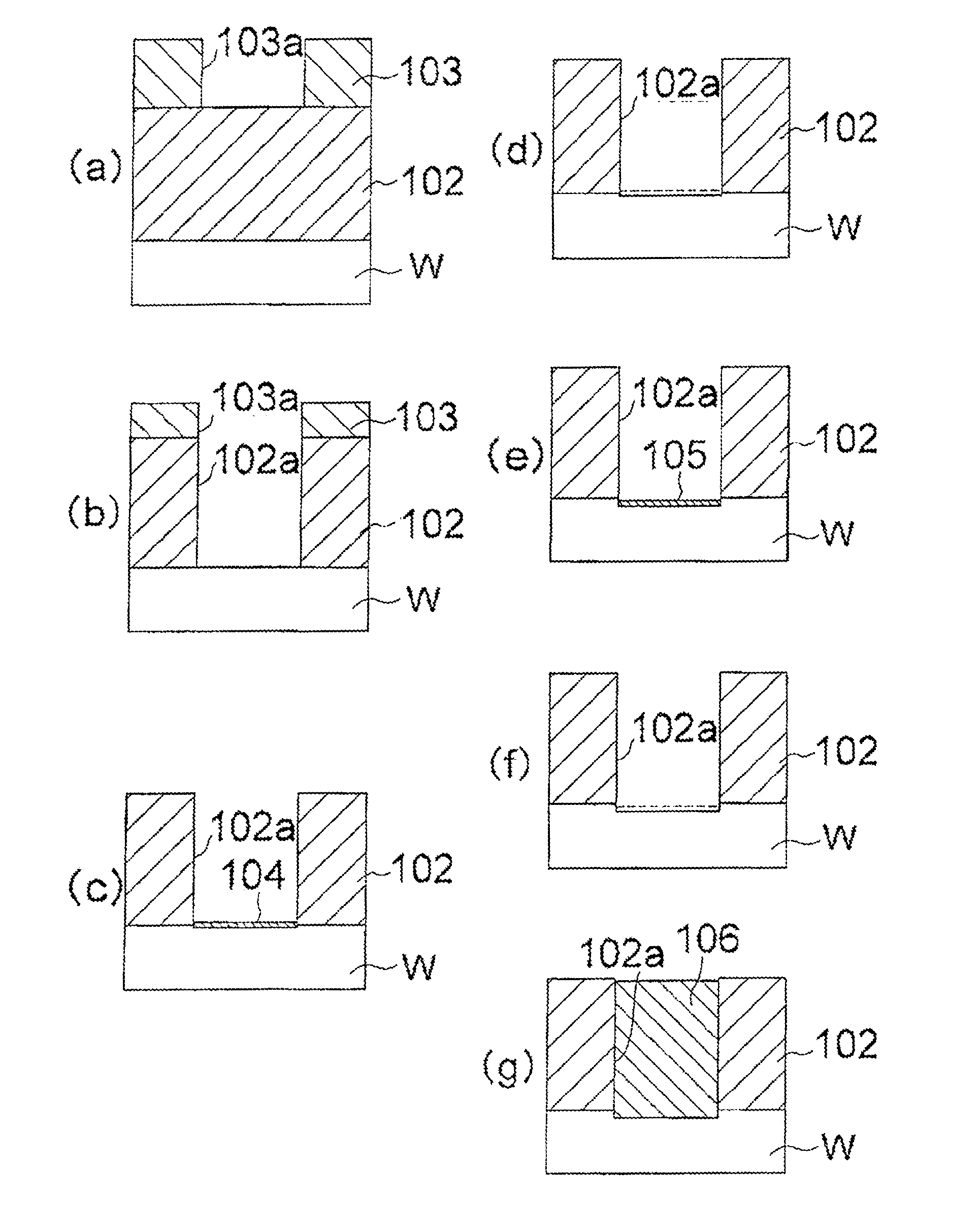
[0033]The present invention will be described in detail by explaining exemplary embodiments of the invention with reference to the attached drawings. Like reference numerals in the drawings denote like elements.
[0034]
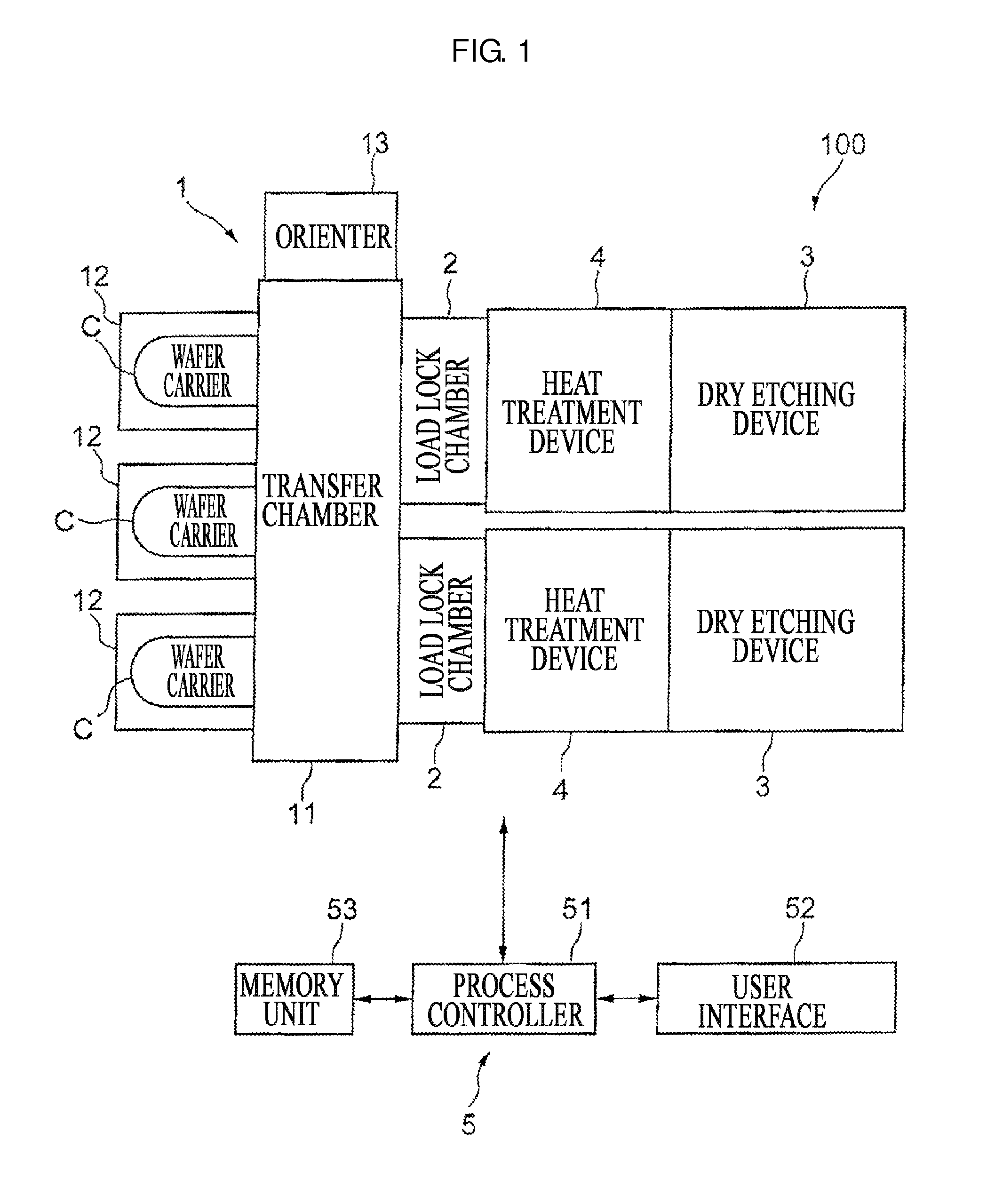
[0035]FIG. 1 is a plan view of a system 100 for etching a substrate, according to an embodiment of the present invention. The system 100 includes a delivering unit 1 for carrying a semiconductor wafer (referred to as a wafer hereinafter) into or out of the system 100, a load lock chamber 2 constituted adjacent to the delivering unit 1, a dry etching device 3 for performing dry etching on the wafer, a heat treatment device 4 for performing heat treatment on the wafer having been dry etched, and a control unit 5 for controlling each element of the system 100.
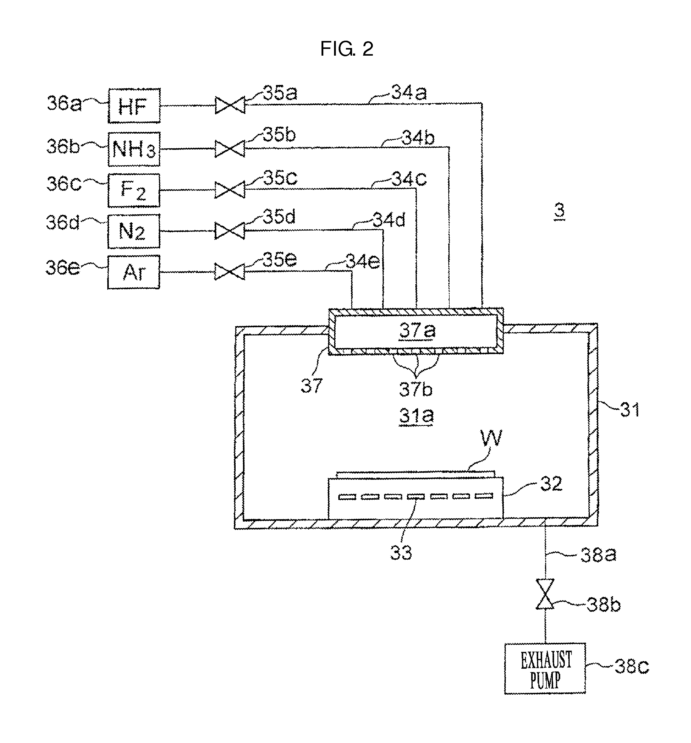
[0036]Two of the load lock chambers 2, two of the dry etching devices 3, and two of the heat treatment devices 4 are constituted in the etching system 100 of the embodiment illustrated in FIG. 1. The load lock chamber...
PUM
| Property | Measurement | Unit |
|---|---|---|
| aaaaa | aaaaa |
Abstract
Description
Claims
Application Information
 - Generate Ideas
- Intellectual Property
- Life Sciences
- Materials
- Tech Scout
- Unparalleled Data Quality
- Higher Quality Content
- 60% Fewer Hallucinations
Browse by: Latest US Patents, China's latest patents, Technical Efficacy Thesaurus, Application Domain, Technology Topic, Popular Technical Reports.
© 2025 PatSnap. All rights reserved.Legal|Privacy policy|Modern Slavery Act Transparency Statement|Sitemap|About US| Contact US: help@patsnap.com