Artifical dielectric composites by a direct-write method

a dielectric composite and direct-write technology, applied in the field of dielectric composites, can solve the problems of composites beset by their own technical difficulties, difficult to achieve, and heavy materials, and achieve the effects of less expensive production, reduced cost, and lighter weigh

Inactive Publication Date: 2010-09-30
THE UNITED STATES OF AMERICA AS REPRESENTED BY THE SECRETARY OF THE NAVY
View PDF15 Cites 1 Cited by
  • Summary
  • Abstract
  • Description
  • Claims
  • Application Information

AI Technical Summary

Benefits of technology

[0007]The present invention has many advantages over the prior art. As compared to current RAM products, this invention is both less expensive to produce and lighter in weight. As compared to designs for dielectric RAM, the present invention shares the same advantage of light weight, while significantly reducing the cost. No advanced materials are required. This invention also removes one of the main obstacles to development of fiber-filled dielectrics, namely, the lack of uniformity. Using the technique of the present invention, it is easy to generate absolutely uniform patterns of metal tracings. As compared to known fiber-based dielectrics, it is also easy to vary the length, aspect ratio, shape, orientation, distribution, and other properties of a composite.

Problems solved by technology

These materials are both very heavy and very costly, two key limitations to their adoption for many applications.
While successful in many ways, these composites are beset by their own technical difficulties.
Uniformity and consistency, critical attributes for a successful RAM, are difficult to achieve with fiber-filled composites as mixing and distribution of the fibers is opposed by the natural tendency of the fibers to clump.

Method used


Image

  • Artifical dielectric composites by a direct-write method
  • Artifical dielectric composites by a direct-write method
  • Artifical dielectric composites by a direct-write method

Examples


Embodiment Construction

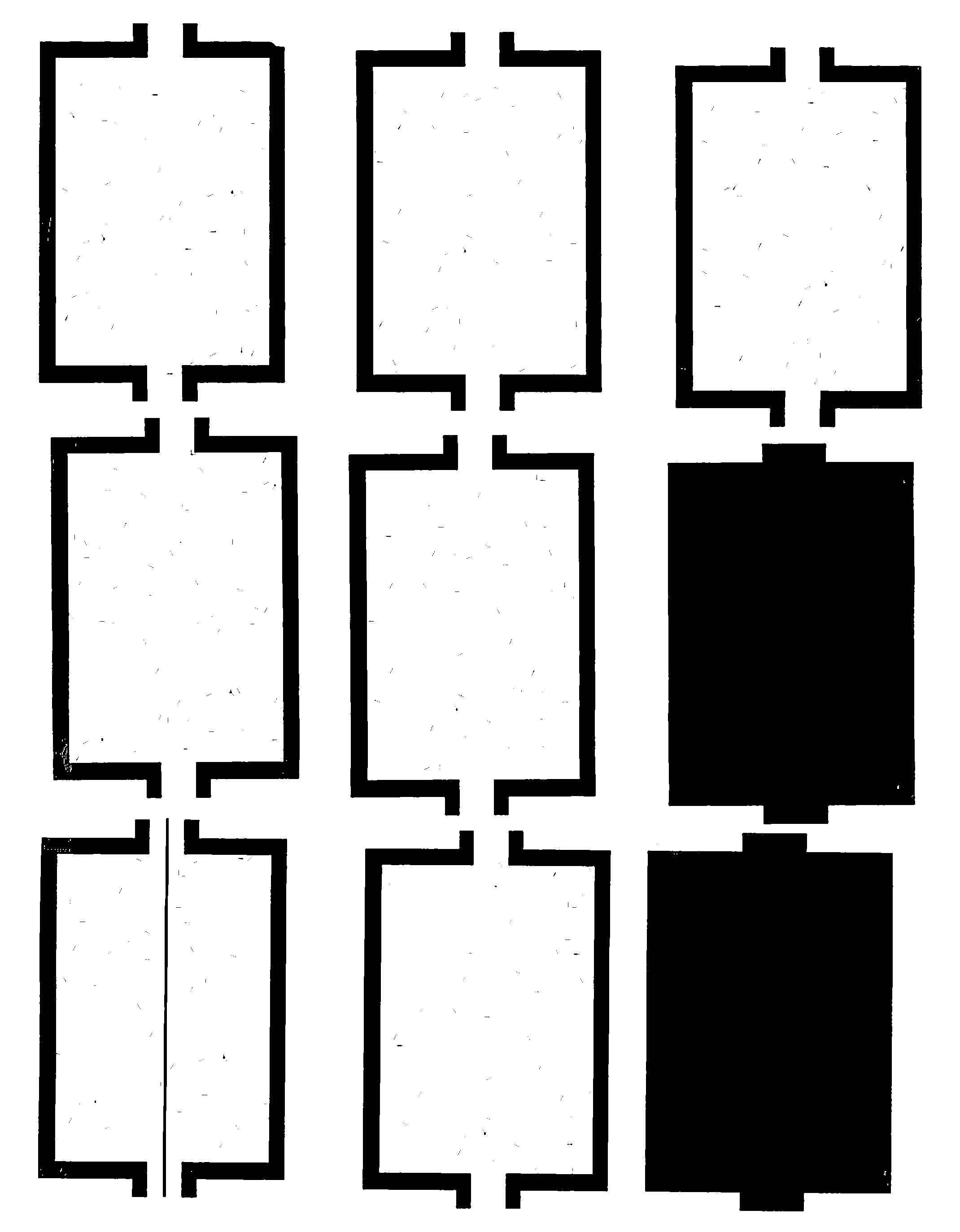
[0016]According to the present invention, a material suitable for use in composites applicable to various electromagnetic needs is prepared using a direct-write method. An electrically non-conducting pattern, typically comprising palladium, is printed onto an electrically non-conducting substrate, typically based on a textile such as paper, using a direct-write device. The pattern is then covered with an electrically conducting coating, typically by immersing the substrate in an electroless plating solution. Metals available for electroless deposition include nickel, gold, silver, palladium, cobalt, iron, and copper. The patterned conductive lines modify the electromagnetic parameters of the material. By controlling the complex dielectric constant of a material, it is possible to construct RF-absorbing composites.

[0017]The present invention uses a direct-write device, such as a commercial inkjet printer. Other types of writing devices may be used, including other inkjet technologies...


PUM

PropertyMeasurementUnit
sizesaaaaaaaaaa
temperatureaaaaaaaaaa
dielectricaaaaaaaaaa

Abstract

The present invention is generally directed to an artificial dielectric composite having an electrically non-conducting substrate, an electrically non-conducting pattern on the substrate, and an electrically conducting coating on the pattern. The substrate may be a textile such as paper. The electrically non-conducting pattern may comprise palladium. A direct-write device, such as an inkjet printer, may be used to print the pattern onto the substrate. The electrically conducing coating may comprise nickel, gold, palladium, cobalt, iron, copper, or any combination thereof. Also disclosed is the related method of making the artificial dielectric composite.

Description

BACKGROUND OF THE INVENTION[0001]1. Field of the Invention[0002]The present invention relates generally to dielectric composites and, more particularly, to artificial dielectrics prepared by a direct-write method.[0003]2. Description of the Prior Art[0004]Radar absorbing material (RAM) currently in military and commercial use are typically composed of high concentrations of iron powders in a polymer matrix. These materials are both very heavy and very costly, two key limitations to their adoption for many applications.[0005]Various attempts to overcome these problems have involved the creation of artificial dielectrics, including ones based on conductive fiber-filled composites. While successful in many ways, these composites are beset by their own technical difficulties. Uniformity and consistency, critical attributes for a successful RAM, are difficult to achieve with fiber-filled composites as mixing and distribution of the fibers is opposed by the natural tendency of the fibers ...

Claims


Application Information

Patent Timeline
Patent Type & Authority Applications(United States)
IPC IPC(8): H01Q17/00B05D5/12
CPCH01Q1/00
Inventor ZABETAKIS, DANIEL
Owner THE UNITED STATES OF AMERICA AS REPRESENTED BY THE SECRETARY OF THE NAVY
Why Eureka
Try Eureka