Pixel array, liquid crystal display panel, and electro-optical apparatus

a liquid crystal display panel and pixel array technology, applied in static indicating devices, non-linear optics, instruments, etc., can solve the problem of color washout not being effectively solved, and achieve the effect of improving image quality and low parasitic capacitan

Active Publication Date: 2010-10-07
AU OPTRONICS CORP
View PDF4 Cites 45 Cited by
  • Summary
  • Abstract
  • Description
  • Claims
  • Application Information

AI Technical Summary

Benefits of technology

[0026]As described above, in the present invention, the first scan line in each sub-pixel is disposed between the first pixel electrode and the second pixel electrode. Accordingly, the pixel array in the present invention has lower parasitic capacitance and accordingly provides a better image quality.

Problems solved by technology

As a result, the problem of color washout cannot be effectively resolved.

Method used


Image

  • Pixel array, liquid crystal display panel, and electro-optical apparatus
  • Pixel array, liquid crystal display panel, and electro-optical apparatus
  • Pixel array, liquid crystal display panel, and electro-optical apparatus

Examples


first embodiment

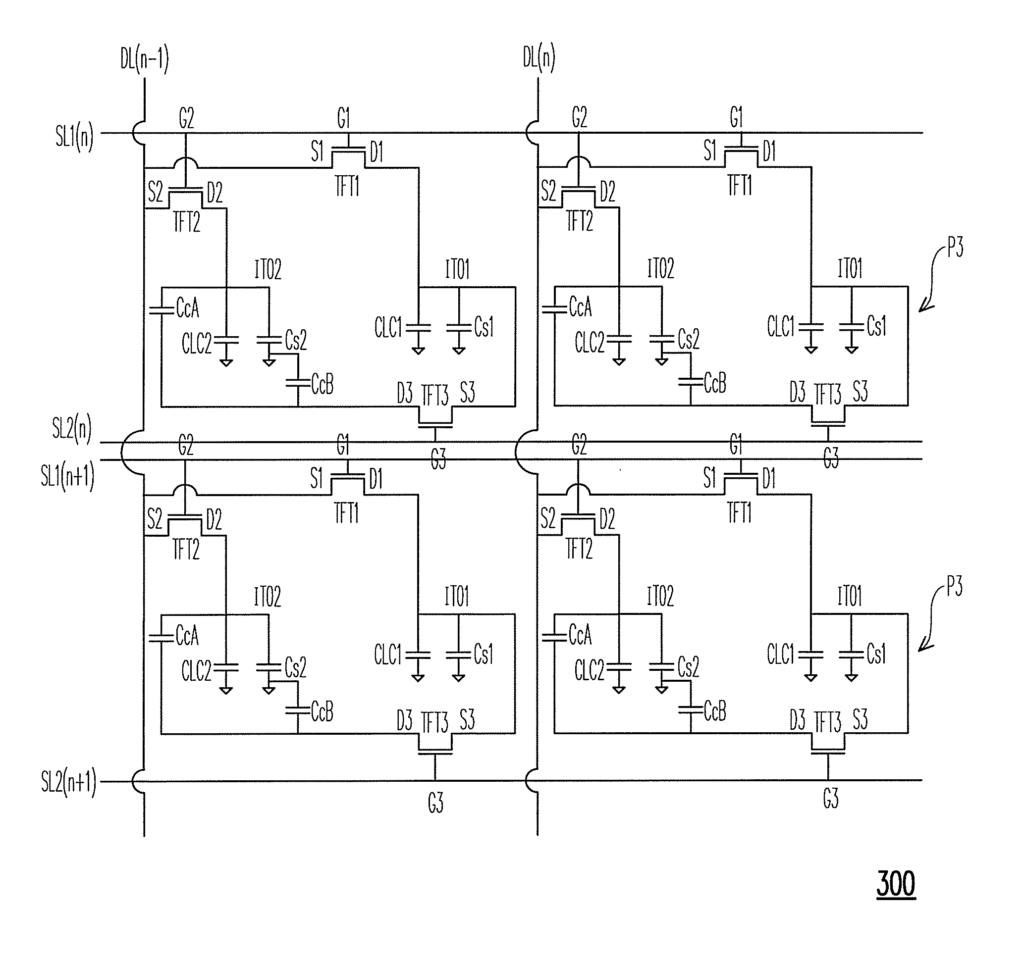
[0044]FIG. 3A is an equivalent circuit diagram of a pixel array according to the first embodiment of the present invention, FIG. 3B is a diagram of a pixel array according to the first embodiment of the present invention, and FIG. 3B′ is a cross-sectional view of the pixel array in FIG. 3B along line A-A′. Referring to FIG. 3A and FIG. 3B, the pixel array 300 of the present embodiment includes a plurality of first scan lines SL1, a plurality of second scan lines SL2, a plurality of data lines DL, and a plurality of sub-pixels P3. The first scan lines SL1 include first scan lines SL1(1)˜SL1(n+1), the second scan lines SL2 include second scan lines SL2(1)˜SL2(n+1), and the data lines DL include data lines DL(1)˜DL(n). Only some of the first scan lines SL1, some of the second scan lines SL2, and some of the data lines DL are illustrated in FIG. 3A and FIG. 3B.

[0045]Each of the second scan lines SL2 is located between adjacent two first scan lines SL1, and the data lines DL are substant...

second embodiment

[0058]FIG. 5A is an equivalent circuit diagram of a pixel array according to the second embodiment of the present invention, FIG. 5B is a diagram of a pixel array according to the second embodiment of the present invention, FIG. 5B′ is a cross-sectional view of the pixel array in FIG. 5B along line B-B′, and FIG. 5C and FIG. 5D are respectively diagrams of a single sub-pixel in FIG. 5B. Referring to FIGS. 5A˜5C, the pixel array 400 in the present embodiment is similar to the pixel array 300 in the first embodiment, and the major difference between the two embodiments is that in the pixel array 400, the second pixel electrode ITO2 in each of the sub-pixels P4 is located between the first scan line SL1 and the second scan line SL2. Specifically, the third source S3 of the third thin film transistor TFT3 extends across the second pixel electrode ITO2 and electrically connected to the first drain D1 directly (as shown in FIG. 5C). Accordingly, a parasitic capacitance Cx2 is generated be...

third embodiment

[0061]FIG. 7 is a diagram of a polymer stabilized alignment liquid crystal display (PSA-LCD) panel in the present invention. Referring to FIG. 7, in the present embodiment, the PSA-LCD panel 600 includes a first substrate 610, a second substrate 620, two PSA layers 630 and 640, and a liquid crystal layer 650. The first substrate 610 has a pixel array (300 or 400) in the first or second embodiment described above, the second substrate 620 is disposed above the first substrate 610, and the two PSA layers 630 and 640 are respectively disposed on the first substrate 610 and the second substrate 620. Besides, the liquid crystal layer 650 is disposed between the two PSA layers 630 and 640. It should be noted that the liquid crystal layer 650 is made of a liquid crystal material containing monomers which can be polymerized by an energy source. When the energy source (for example, an ultraviolet ray) is supplied to the liquid crystal layer 650, the monomers are respectively polymerized on t...


PUM

PropertyMeasurementUnit
line widthaaaaaaaaaa
sizeaaaaaaaaaa
voltageaaaaaaaaaa

Abstract

A pixel array including first scan lines, second scan lines, data lines, and sub-pixels is provided. Each sub-pixel includes a first switch, a second switch, a first pixel electrode electrically connected to the first switch, a second pixel electrode electrically connected to the second switch, a third switch, and common lines connected with each other and disposed under the first and the second pixel electrode. The first and the second switch are electrically connected to the same first scan line and data line. The first scan line is located between the first and second pixel electrode. The third switch is electrically connected to the second scan line and the first pixel electrode and has a floating terminal. The floating terminal is capacitively coupled to the second pixel electrode to form a first capacitor and capacitively coupled to the common line under the second pixel electrode to form a second capacitor.

Description

CROSS-REFERENCE TO RELATED APPLICATION[0001]This application claims the priority benefit of Taiwan application serial no. 98111072, filed on Apr. 2, 2009. The entirety of the above-mentioned patent application is hereby incorporated by reference herein and made a part of specification.BACKGROUND OF THE INVENTION[0002]1. Field of the Invention[0003]The present invention generally relates to a pixel array, and more particularly, to a pixel array with good display quality.[0004]2. Description of Related Art[0005]In recent years, the size of liquid crystal display (LCD) has been increased constantly. As a result, techniques for resolving the viewing angle problem in large-sized LCDs have been improved constantly. Multi-domain vertical alignment (MVA) LCD panel and advanced MVA (AMVA) LCD panel are two major wide viewing angle techniques among all LCD techniques. Since the AMVA LCD panel can effectively resolve the color washout problem in the MVA LCD panel, the AMVA LCD panel provides a...

Claims


Application Information

Patent Timeline
Patent Type & Authority Applications(United States)
IPC IPC(8): G02F1/1368G02F1/1337
CPCG02F1/13624G02F2001/134345G02F2001/13606G09G2320/0223G09G2300/0443G09G2300/0809G09G3/3659G02F1/134345G02F1/13606
Inventor TING, TIEN-LUNCHEN, CHIEH-WEIWANG, CHIH-HAWCHIU, CHUNG-YIHSU, WEN-HAOSU, JENN-JIA
Owner AU OPTRONICS CORP
Why Eureka
Try Eureka