Chip part manufacturing method and chip parts
a technology of chip parts and manufacturing methods, applied in the direction of resist details, inductances, printed circuit aspects, etc., can solve the problems of parts not being smoothly fed, broken or cracked chip parts, etc., to suppress chip rising, smooth feeding, and suppress chip breaking or cracking.
- Summary
- Abstract
- Description
- Claims
- Application Information
AI Technical Summary
Benefits of technology
Problems solved by technology
Method used
Image
Examples
embodiment 1
Preferred Embodiment 1
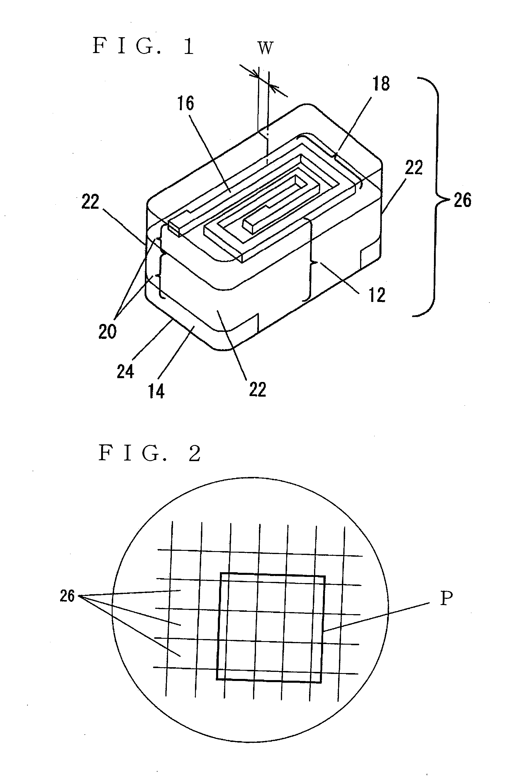
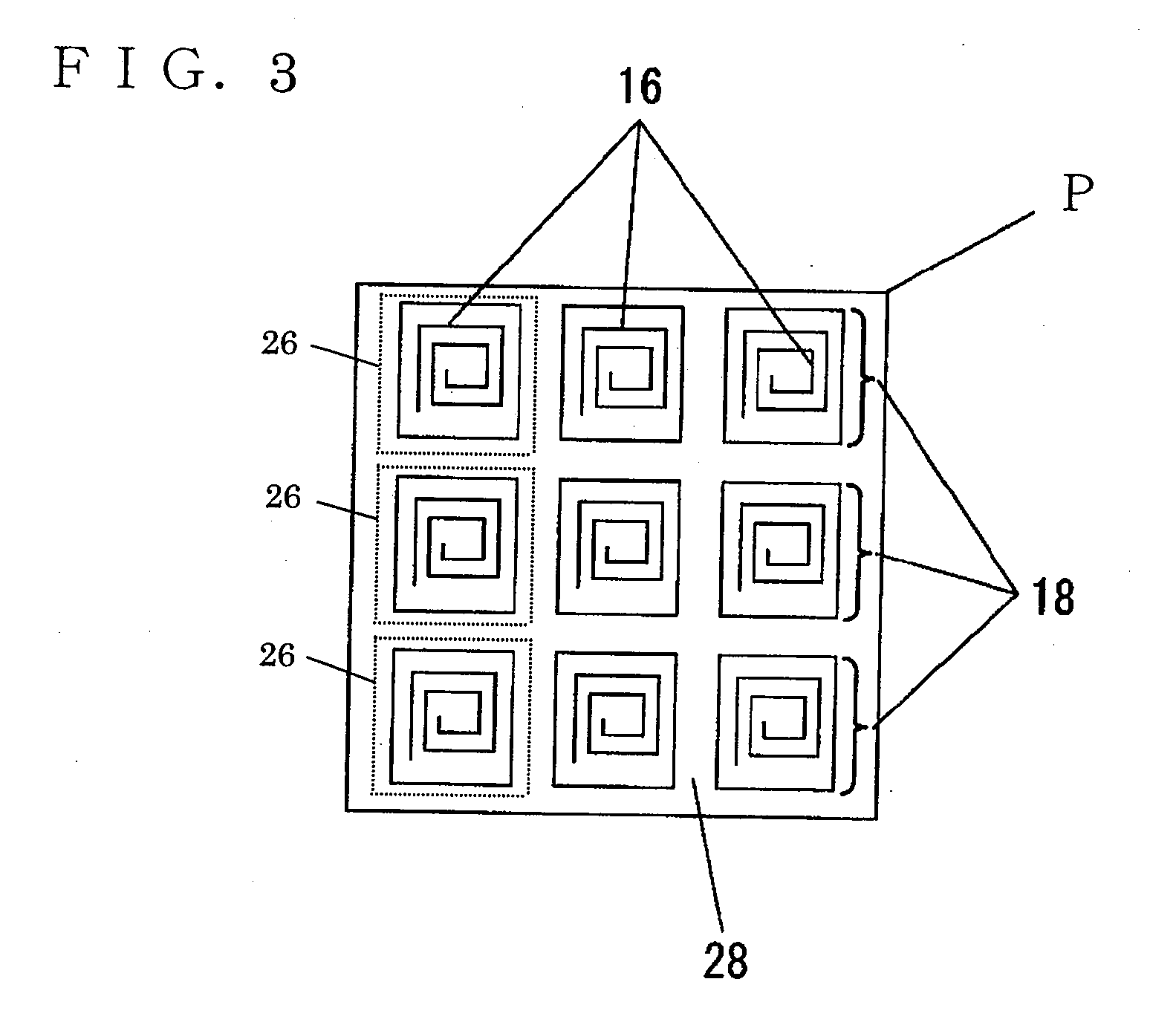
[0048]FIG. 1 is a perspective view of a chip part in the preferred embodiment 1. FIG. 2 is a plan view showing a state of a plurality of chip parts connected to each other. FIG. 3 is an enlarged view of portion P in FIG. 2. FIG. 4A to FIG. 4F are process diagrams showing a chip parts manufacturing process of the present invention.
[0049]In FIG. 1, chip part 26 in one preferred embodiment of the present invention is shown, for example, as a chip coil part. Chip part 26 comprises element 12 which is generally squared and transparent, electrode 14 disposed at the bottom of element 12, and coil section 18 formed by spiral metal layer 16 buried in element 12. Element 12 is formed by laminating insulating resin layers 20 formed from a photosensitive resin material obtained by hardening photosensitive resin.
[0050]Also, first corner 22 of chip part 26 is generally arcuate, which is formed at element 12, in a position perpendicular to the mounting surface. Second corner ...
embodiment 2
Preferred Embodiment 2
[0078]FIG. 5A to FIG. 5G show another manufacturing process of chip part 26 of the present invention. Since FIG. 1, FIG. 2 and FIG. 3 used in the preferred embodiment 1 can be used in the preferred embodiment 2 as well, the detailed description is omitted. As compared with the preferred embodiment 1, one more manufacturing process is shown in the preferred embodiment 2. Also, it is clear at first sight that FIG. 5A to FIG. 5G are similar to FIG. 4A to FIG. 4F.
[0079]FIG. 5A shows a step of forming an electrode. At the top of FIG. 5A, a release layer (not shown) is formed on one main surface of substrate 30, and insulating resin layer 20 having electrode void portion 34 is formed by a photolithography process on the upper surface of the release layer. The release layer can be, for example, formed by using release resist. In the case of forming a release layer, the chip parts described later can be easily separated from the frame-like connection and it is possible...
PUM
 Abstract
Description
Claims
Application Information


