
Wrapped solar cel

a solar cel and solar cell technology, applied in the field of photovoltaic devices, can solve the problems of poor carrier transport, inability to match inorganic thin film photovoltaics in terms of efficiencies, and still associated with organic photovoltaics

Inactive Publication Date: 2010-10-14
CURRAN SEAMUS
View PDF3 Cites 8 Cited by
  • Summary
  • Abstract
  • Description
  • Claims
  • Application Information

AI Technical Summary

Benefits of technology

The patent describes a photovoltaic device that has a vertical geometry and can be made in various shapes such as a cylinder, square, oval, rope, ribbon, oblong, and rectangular. The device includes a photovoltaic cell with at least one semiconductor, a high work-function electrode, and a low work-function electrode. It may also have additional layers such as a protective layer, substrate layer, band bending layer, and electron transporting layer. The method of making the device involves layering the photovoltaic cell and additional layers and wrapping them from the inside out. The technical effects of this patent include improved photovoltaic device performance and flexibility in device shape and design.

Problems solved by technology

Although the first plastic solar cells were fabricated about twenty years ago, the ability to match inorganic thin film photovoltaics in terms of efficiencies has failed.
Clearly, there are fundamental problems still associated with organic photovoltaics that have to be addressed before they can advance to the levels achieved by their inorganic counterparts.
Charge Carrier Transport: Polymers and polymer composites can convert almost all resonant light into charge earners (electrons and holes or excitons), but carrier transport is poor.
First, the exciton generated can only travel very short distances, typically about 50 nm, before being recombined and secondly organic based photovoltaics possess poor mobilities and conductivities.
Consequently, polymer composite devices fabricated can only be made from ultra-thin semiconductor films (less than 250 nm).
Transparency Due to the necessity to have very thin films as a consequence of poor carrier transport properties, significant light is lost due to transparency.
The issues inherent with organic based devices are obviously different than inorganics, yet persisting with the same design does not address and solve these problems.
Thus, fiat panel designs like those generally used for the last twenty years are not efficient for organic photovoltaics and a new and more efficient design would be desirable.

Method used


Image

  • Wrapped solar cel
  • Wrapped solar cel
  • Wrapped solar cel

Examples


Embodiment Construction

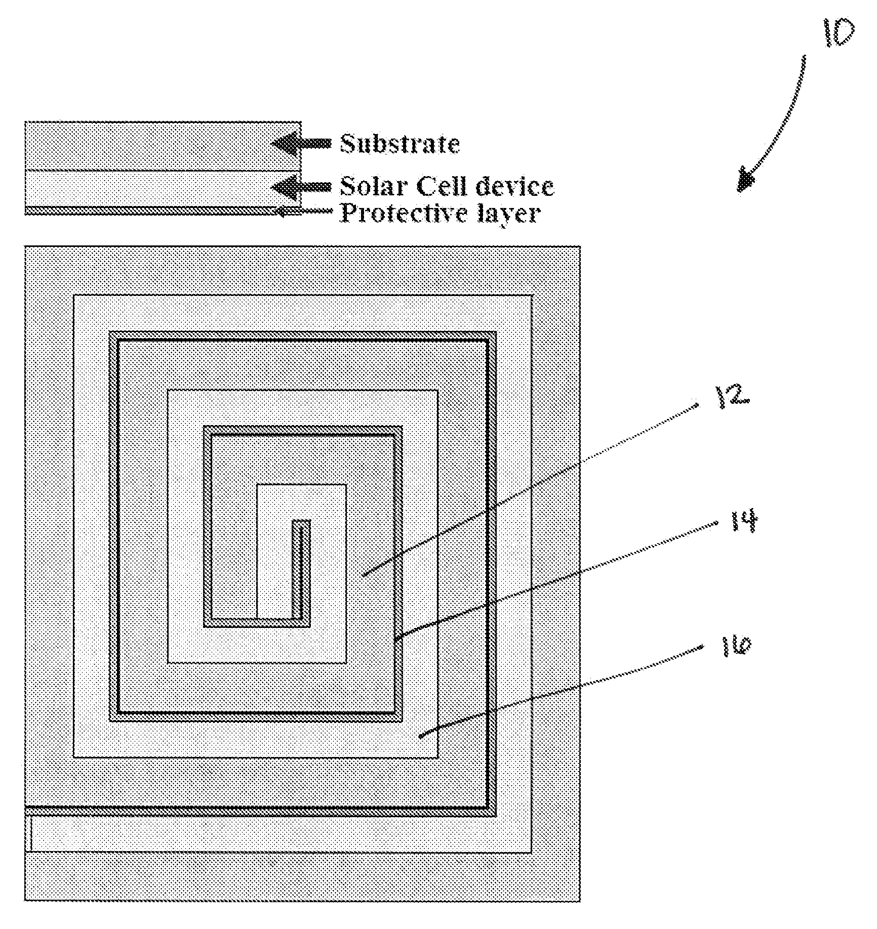
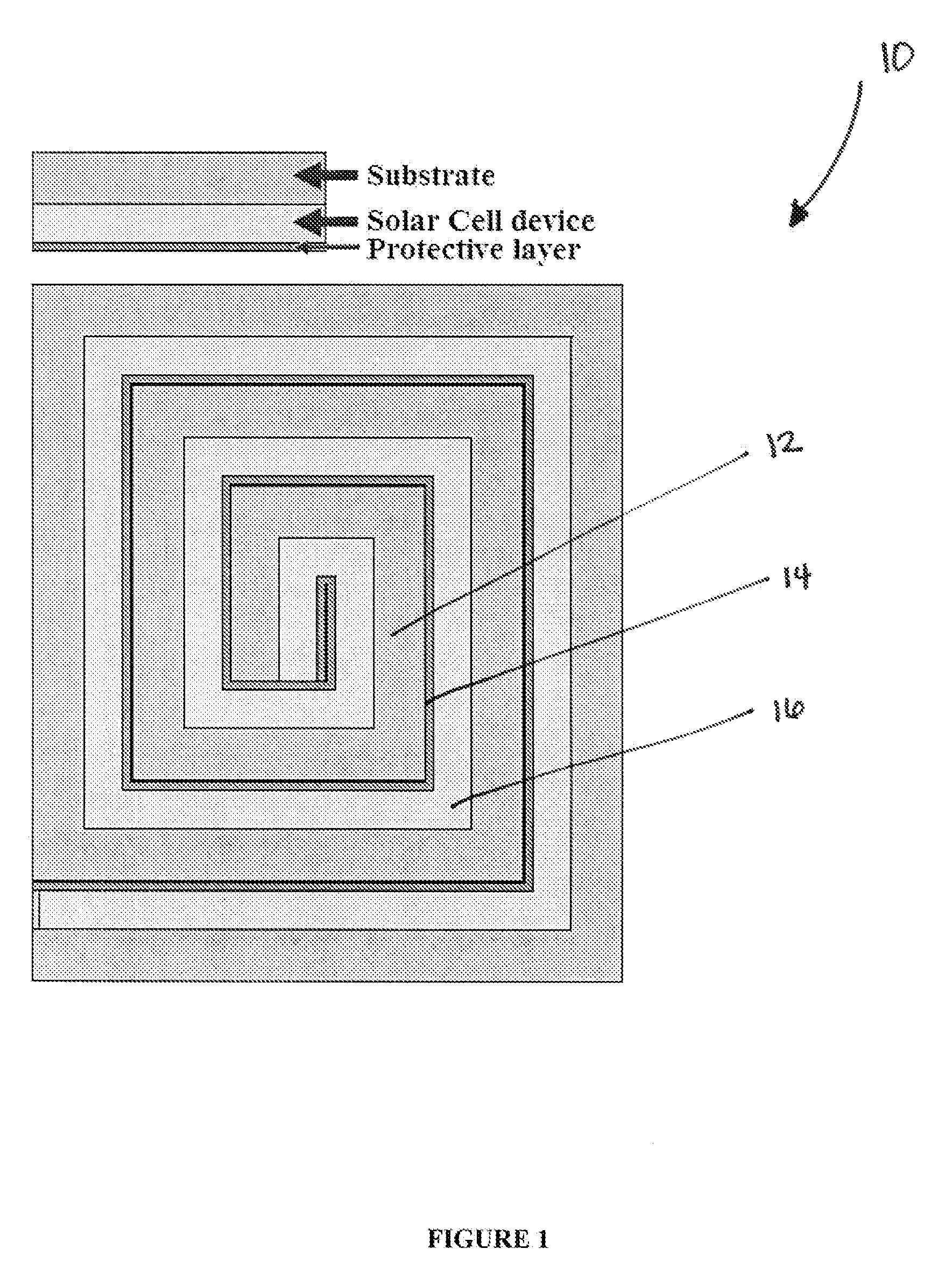
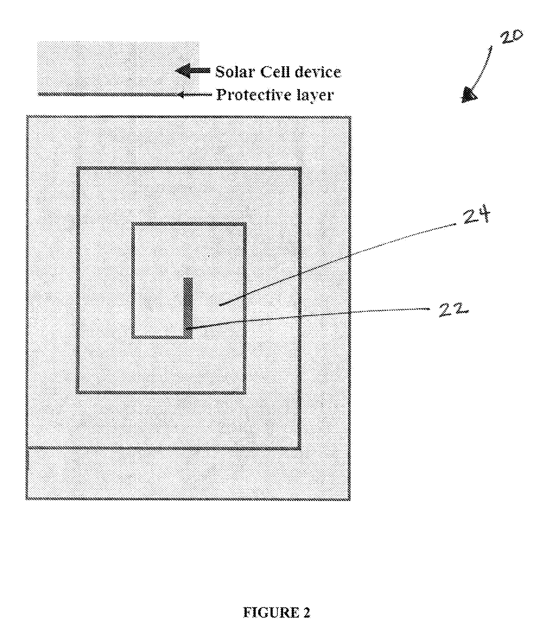
[0028]The present disclosure describes a photovoltaic device design that consists of one or more organic layers successively wrapped up in thin-film design. The device and method according to the present disclosure enable light and charge to be managed in such a way that successive organic (hybrid, doped or heterojunction) layers can be printed and subsequently wrapped in a variety of shapes including a cylinder, square, oval, rope, ribbon, oblong or rectangular geometry of successive device layers from small on the inside to large on the outside.

[0029]The design of the photovoltaic device according to the present disclosure allows the maintenance of a thin semiconductor film without suffering from substantial transparency issues. Also, the design of the photovoltaic device enables light to be contained within the various layers until most of the resonant (resonant to the semiconductor) light is absorbed. By wrapping the layers around, the photovoltaic device can have a vertical geo...


PUM

PropertyMeasurementUnit
band gapaaaaaaaaaa
thicknessesaaaaaaaaaa
thickaaaaaaaaaa

Abstract

A photovoltaic device comprising a photovoltaic cell and at least one layer, the photovoltaic ceil and at least one layer wrapped from the inside out to form the photovoltaic device having a vertical geometry is provided. The photovoltaic device can be a variety of shapes. These shapes include a cylinder, square, oval, rope, ribbon, oblong and rectangular. Generally, the photovoltaic cell has at least on semiconductor, a hirfi work-function electrode and a low work-function electrode.

Description

RELATED APPLICATION INFORMATION[0001]This patent application takes the priority of U.S. Provisional Application No. 60 / 950,528, filed in the U.S. Patent and Trademark Office on Jul. 18, 2007. The entire contents are incorporated herein by reference.FIELD OF THE INVENTION[0002]The present invention generally relates to a photovoltaic device and method of production of the photovoltaic device and more particularly, to a photovoltaic device that manages both charge and optics in an organic photovoltaic cell with multiple wrapped thin film layers, which are vertically oriented.BACKGROUND OF THE INVENTION[0003]Plastic (polymer) materials have, for the last two decades, received considerable attention as potentially a new material of choice for photonic based electronics. Classically, optical properties of plastics and their composite derivatives have great potential as they can convert almost all resonant light into energy (charge carrier generation), their absorption can be tailored to ...

Claims


Application Information

Patent Timeline
Patent Type & Authority Applications(United States)
IPC IPC(8): H01L31/0256H01L31/18H01L31/02
CPCB82Y10/00H01L51/0004H01L51/0038H01L51/0046H01L51/0048Y02E10/549H01L51/4206H01L51/424H01L51/4253H01L51/447H01L51/0097Y02P70/50H10K71/13H10K85/114H10K85/211H10K85/221H10K77/111H10K30/451H10K30/20H10K30/30H10K30/87H10K30/50
Inventor CURRAN, SEAMUS
Owner CURRAN SEAMUS
Learn More