Semiconductor package to remove power noise using ground impedance

Active Publication Date: 2010-10-14
SAMSUNG ELECTRONICS CO LTD
View PDF2 Cites 14 Cited by
  • Summary
  • Abstract
  • Description
  • Claims
  • Application Information

AI Technical Summary

Benefits of technology

[0007]To prevent high frequency noise, separation of a ground of the analog circuit blocks and a ground of the digital circuit blocks on a circuit substrate has been suggested. However, when an analog ground and a digital ground are sepa

Problems solved by technology

The high frequency components, however, generate significant noise in the analog circuit blocks.
However, when an analog ground and a digital ground are separated from each other and are connected to a system board-level ground and a chipset-level ground, respectively, the number of package ground balls may be increased, and this may consequently increase the size of a semiconductor package.
Also, when the analog ground and the digital ground are separated as described above, a ground may not be provided sta

Method used


Image

  • Semiconductor package to remove power noise using ground impedance
  • Semiconductor package to remove power noise using ground impedance
  • Semiconductor package to remove power noise using ground impedance

Examples


Embodiment Construction

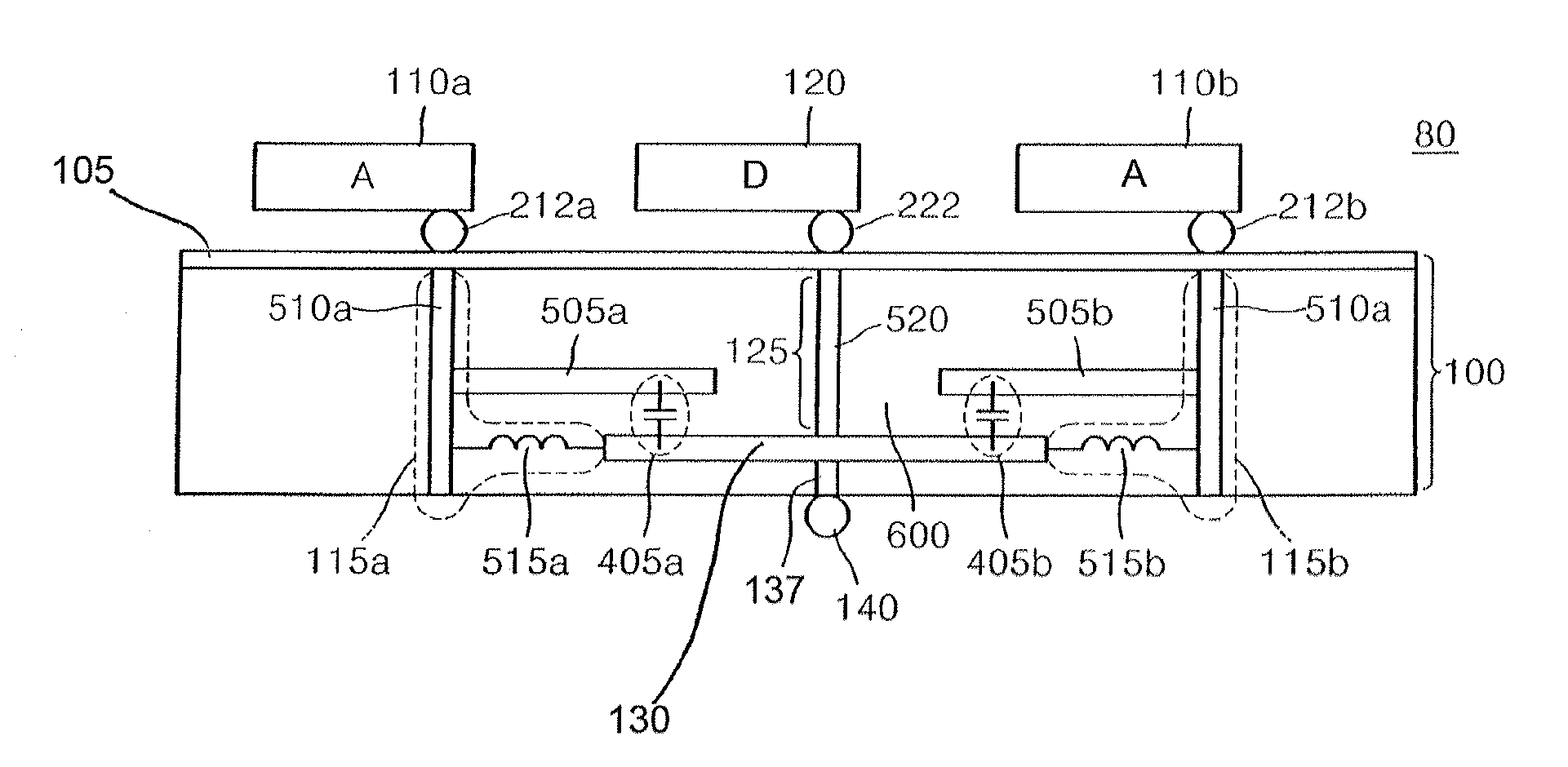
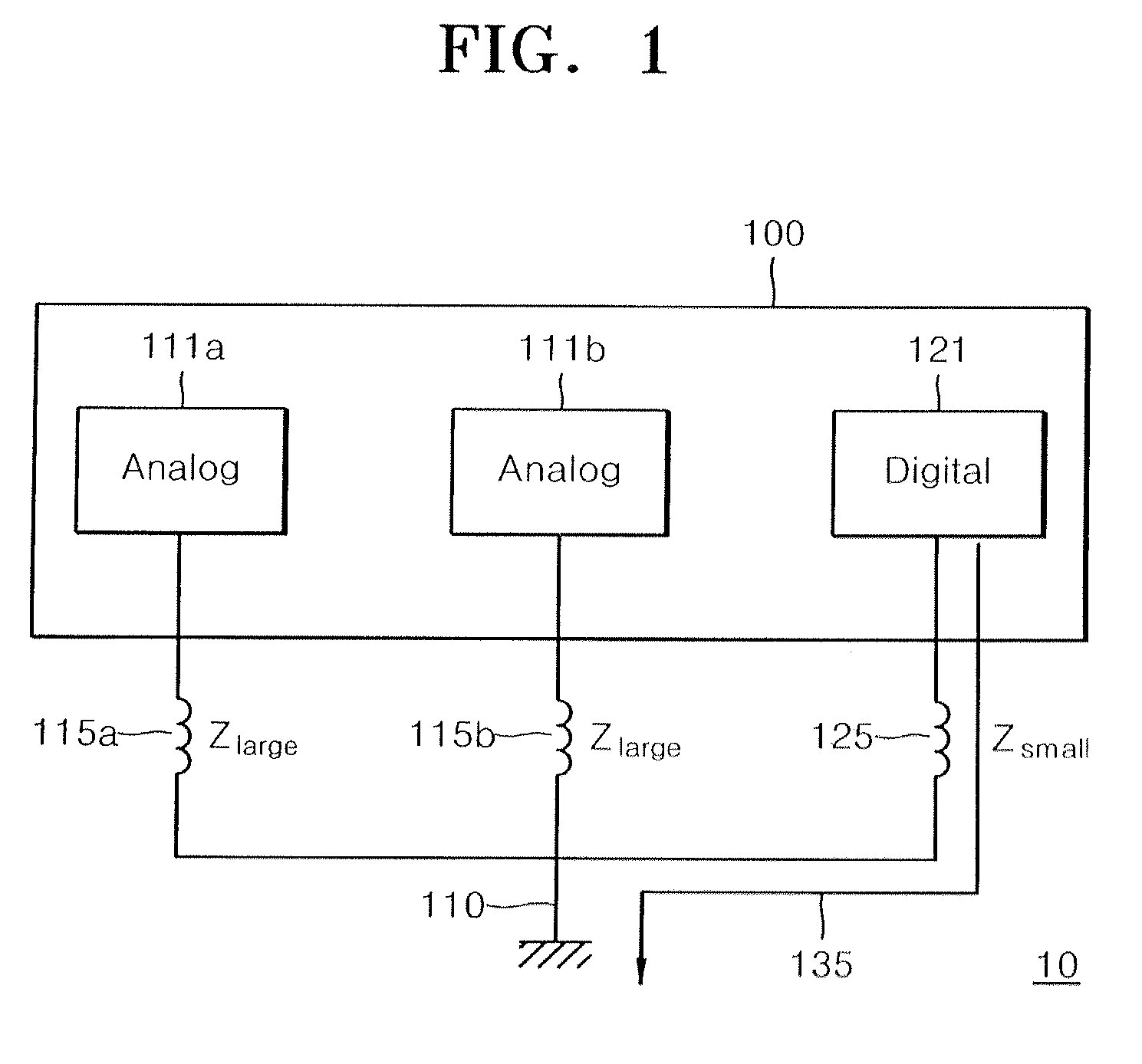
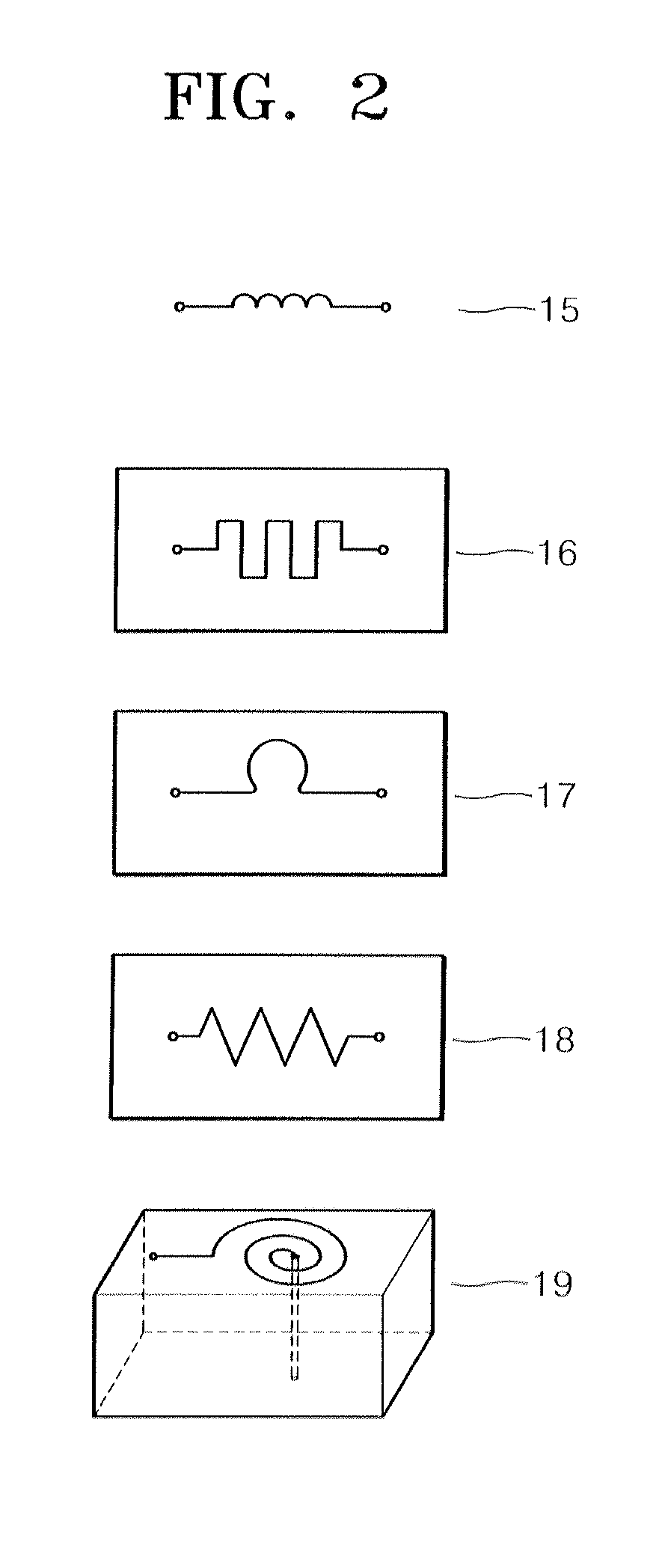
[0043]Reference will now be made in detail to the embodiments of the present general inventive concept, examples of which are illustrated in the accompanying drawings, wherein like reference numerals refer to the like elements throughout. The embodiments are described below in order to explain the present general inventive concept by referring to the figures.

[0044]Detailed illustrative example embodiments are disclosed herein. However, specific structural and functional details disclosed herein are merely representative for purposes of describing example embodiments. This general inventive concept may, however, may be embodied in many alternate forms and should not be construed as limited to only the example embodiments set forth herein.

[0045]The terminology used herein is for the purpose of describing particular embodiments only and is not intended to be limiting of example embodiments. As used herein, the singular forms “a,”“an” and “the” are intended to include the plural forms a...


PUM


Abstract

A semiconductor package removes power noise by using a ground impedance. The semiconductor package includes an analog circuit block, a digital circuit block, an analog ground impedance structure, a digital ground impedance structure, and an integrated ground. The integrated ground and the analog circuit block are electrically connected via the analog ground impedance structure, and the integrated ground and the digital circuit block are electrically connected via the digital ground impedance structure, and an inductance of the analog ground impedance structure is greater than an inductance of the digital ground impedance structure.

Description

CROSS-REFERENCE TO RELATED APPLICATIONS[0001]This application claims the benefit of Korean Patent Application No. 10-2009-0031430, filed on Apr. 10, 2009 in the Korean Intellectual Property Office, the disclosure of which is incorporated by reference herein in its entirety.BACKGROUND[0002]1. Field of the Invention[0003]The general inventive concept relates to a semiconductor package, and more particularly, to a semiconductor package in which an analog circuit block and a digital circuit block are formed in combination.[0004]2. Description of the Related Art[0005]With recent increases in integration of semiconductor devices, semiconductor packages are being developed that include an analog circuit block and a digital circuit block. These semiconductor packages include a plurality of circuit blocks formed on one substrate, including a plurality of analog circuit blocks and digital circuit blocks are formed in combination. For example, analog circuits may include op-amps, sensors, powe...

Claims


Application Information

Patent Timeline
IPC IPC(8): H01L27/06H02B1/20
CPCH01L23/481H01L23/66H01L2924/30107H01L24/48H01L2924/3011H01L25/0655H01L2224/16H01L2224/48091H01L2224/48227H01L2924/01079H01L2924/19041H01L2924/19051H01L2924/00014H01L2924/00H01L2224/45099H01L2224/45015H01L2924/207H01L21/77
Inventor SONG, EUN-SEOKLEE, HEE-SEOKPARK, SUNG-WOO
Owner SAMSUNG ELECTRONICS CO LTD
Why Eureka
Try Eureka