Semiconductor light emitting element, light source using the semiconductor light emitting element, and optical tomography imaging apparatus

a technology of semiconductor light emitting elements and light sources, applied in semiconductor lasers, electric variable regulation, instruments, etc., can solve the problems of increasing the cost of light sources, and achieve the effect of favorable tomographic images and substantial uniform optical intensities

Inactive Publication Date: 2010-10-14
NICHIA CORP
View PDF13 Cites 33 Cited by
  • Summary
  • Abstract
  • Description
  • Claims
  • Application Information

AI Technical Summary

Benefits of technology

[0041]The optical tomography imaging apparatus of the present invention obtains tomographic images employing laser light emitted by a light source apparatus that operates as a variable wavelength laser capable of obtaining substantially uniform optical intensities for various wavelengths. Therefore, favorable tomographic images can be obtained.

Problems solved by technology

Therefore, the optical filters need to be designed and produced, thereby increasing the cost of the light sources.

Method used


Image

  • Semiconductor light emitting element, light source using the semiconductor light emitting element, and optical tomography imaging apparatus
  • Semiconductor light emitting element, light source using the semiconductor light emitting element, and optical tomography imaging apparatus
  • Semiconductor light emitting element, light source using the semiconductor light emitting element, and optical tomography imaging apparatus

Examples


Embodiment Construction

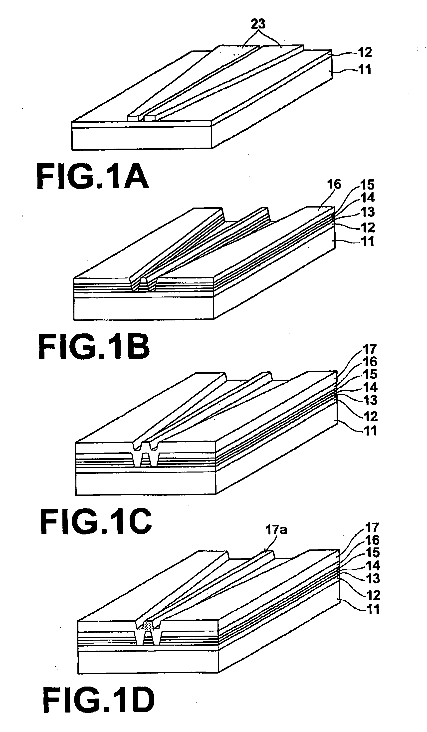
[0055]Hereinafter, embodiments of the present invention will be described with reference to the drawings. FIGS. 1A through 1F are perspective views that illustrate the layer structure and the method for producing a semiconductor light emitting element 1 according to a first embodiment of the present invention.

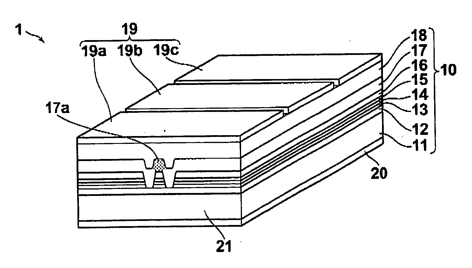
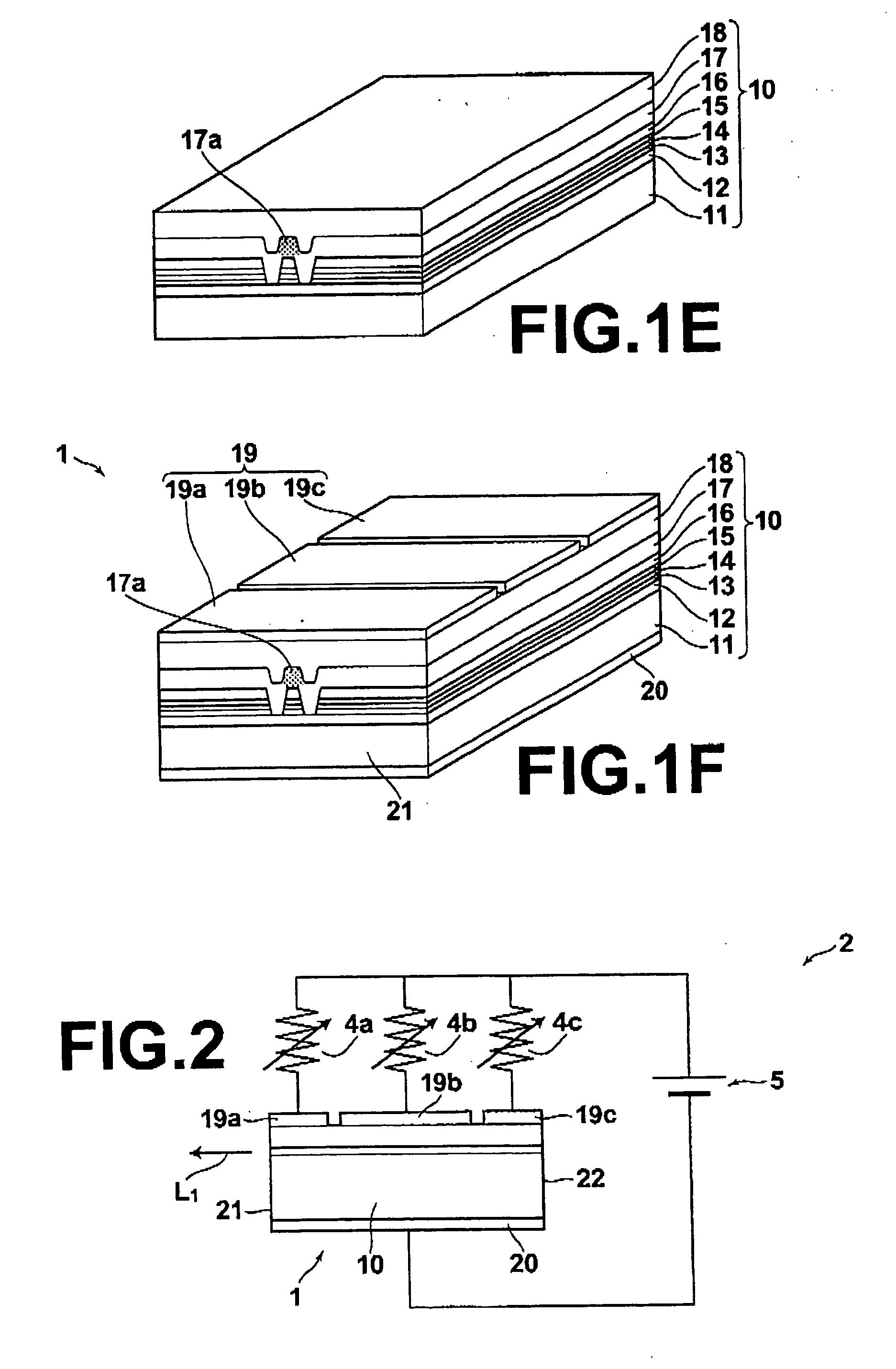
[0056]FIG. 1F illustrates the schematic structure of the semiconductor light emitting element 1 of the first embodiment. The semiconductor light emitting element 1 is of a structure in which the gain wavelength of an active layer changes continuously along a wave guiding direction of light. In the semiconductor light emitting element 1, an electrode layer 19 provided on the upper surface of a layered structure 10 is divided into three electrodes 19a, 19b, and 19c, which are insulated from each other. Each of the divided and insulated electrodes 19a, 19b, and 19c are capable of independently adjusting the amount of current injected thereby.

[0057]The specific structure and the me...


PUM


Abstract

A semiconductor light emitting element is equipped with a layered structure including an active layer, and electrode layers at the upper and lower surfaces thereof. At least one of the upper and lower electrode layers is divided into at least two electrodes, which are separated in the wave guiding direction of light. The active layer is structured to have different gain wavelengths along the wave guiding direction, to emit light having different spectra from each region corresponding to each of the at least two electrodes. The spectral distribution of output light is enabled to be varied by individually varying the current injected by each of the at least two divided electrodes.

Description

BACKGROUND OF THE INVENTION[0001]1. Field of the Invention[0002]The present invention relates to a semiconductor light emitting element, and particularly to a semiconductor light emitting element capable of controlling spectral distribution.[0003]The present invention also relates to a light source apparatus equipped with a semiconductor light emitting element.[0004]The present invention further relates to an optical tomography imaging apparatus.[0005]2. Description of the Related Art[0006]Recently, demand has been growing for low cost multiple wavelength light sources in the fields of optical communications, measurement, and medicine, in which diagnosis and the like are performed using light. A light source for OCT (Optical Coherence Tomography), which is in use for wavelength inspection in optical communications, fiber gyros, OTDR measurement, and opthalmology, is a specific example of such a light source. It is expected that SLD's (Super Luminescent Diodes), which have a high pro...

Claims


Application Information

Patent Timeline
Patent Type & Authority Applications(United States)
IPC IPC(8): G01B9/02H01S5/06H01L33/58H05B37/02
CPCH01L27/15H01L33/0045H01L33/20H01S3/105H01S5/106H01S5/141H01S5/2272H01S5/06255
Inventor ASANO, HIDEKI
Owner NICHIA CORP
Why Eureka
Try Eureka