Semiconductor device and manufacturing method thereof

a technology of semiconductor devices and manufacturing methods, applied in semiconductor devices, basic electric elements, electric devices, etc., can solve problems such as difficulty in suppressing leakage current, restriction on circuit occupancy area reduction, and difficulty in applying desired voltage to source and drain, and achieve the effect of reducing the resistance of the gate electrod

Active Publication Date: 2010-10-21
UNISANTIS ELECTRONICS SINGAPORE PTE LTD
View PDF18 Cites 55 Cited by
  • Summary
  • Abstract
  • Description
  • Claims
  • Application Information

AI Technical Summary

Benefits of technology

[0064]In the semiconductor device according to the fourth aspect of the present invention, in addition to the advantages of the semiconductor device according to the third aspect of the present invention, a metal-semiconductor compound can be adequately on the gate electrode, according to need, to reduce a resistance of the gate electrode.

Problems solved by technology

The progress in miniaturization of the MOS transistor involves problems about difficulty in suppressing a leakage current and restriction on reduction in circuit occupancy area due to a need for ensuring a required current amount.
In this case, if resistances of the source and drain are high, the large ON-current will cause difficulty in applying a desired voltage to the source and drain.

Method used


Image

  • Semiconductor device and manufacturing method thereof
  • Semiconductor device and manufacturing method thereof
  • Semiconductor device and manufacturing method thereof

Examples


Embodiment Construction

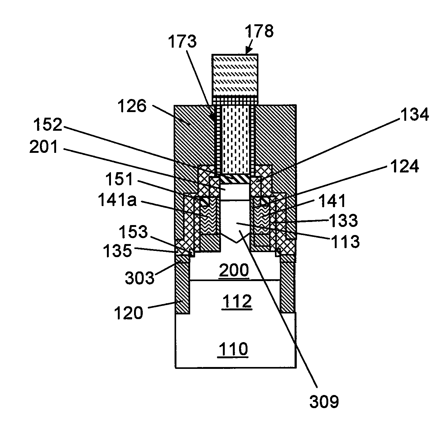
[0148]FIG. 41(a) is a top plan view showing an NMOS (N-channel metal oxide semiconductor)-type SGT obtained by an SGT manufacturing method according to one embodiment of the present invention, and FIG. 41(b) is a sectional view taken along the line A-A′ in FIG. 41(a). With reference to FIGS. 41(a) and 41(b), a structure of the NMOS-type SGT will be described below.

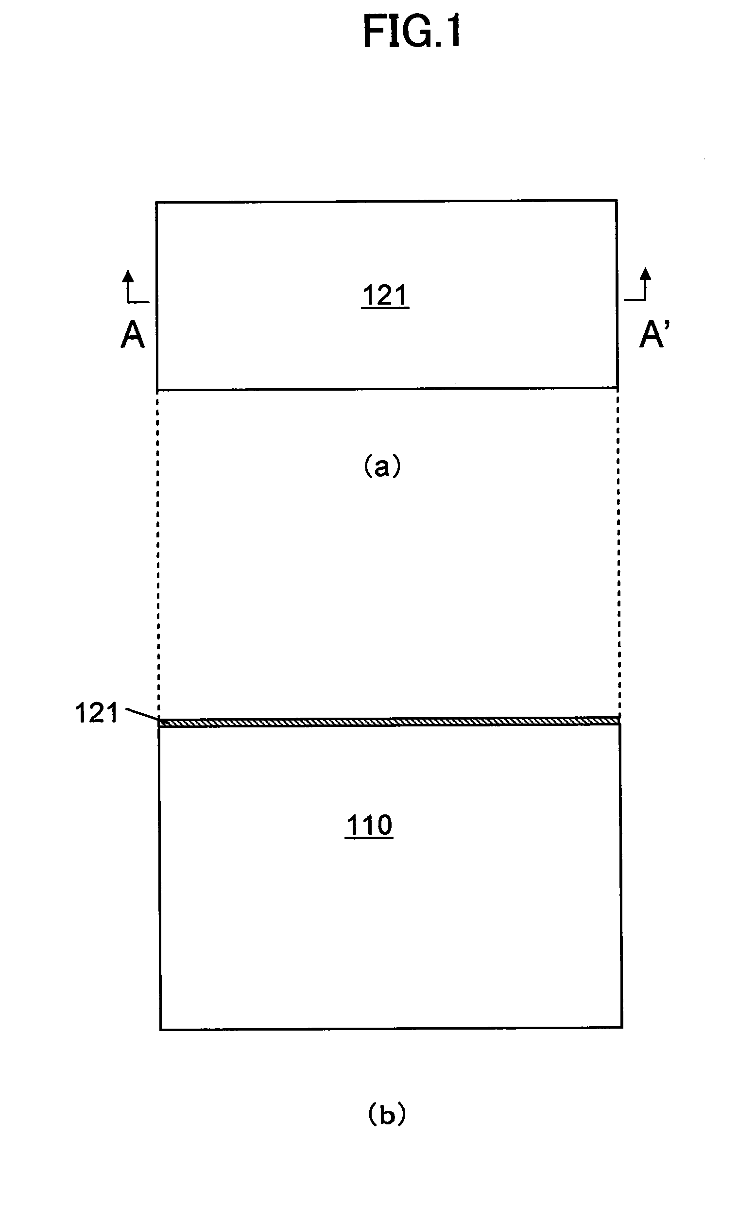
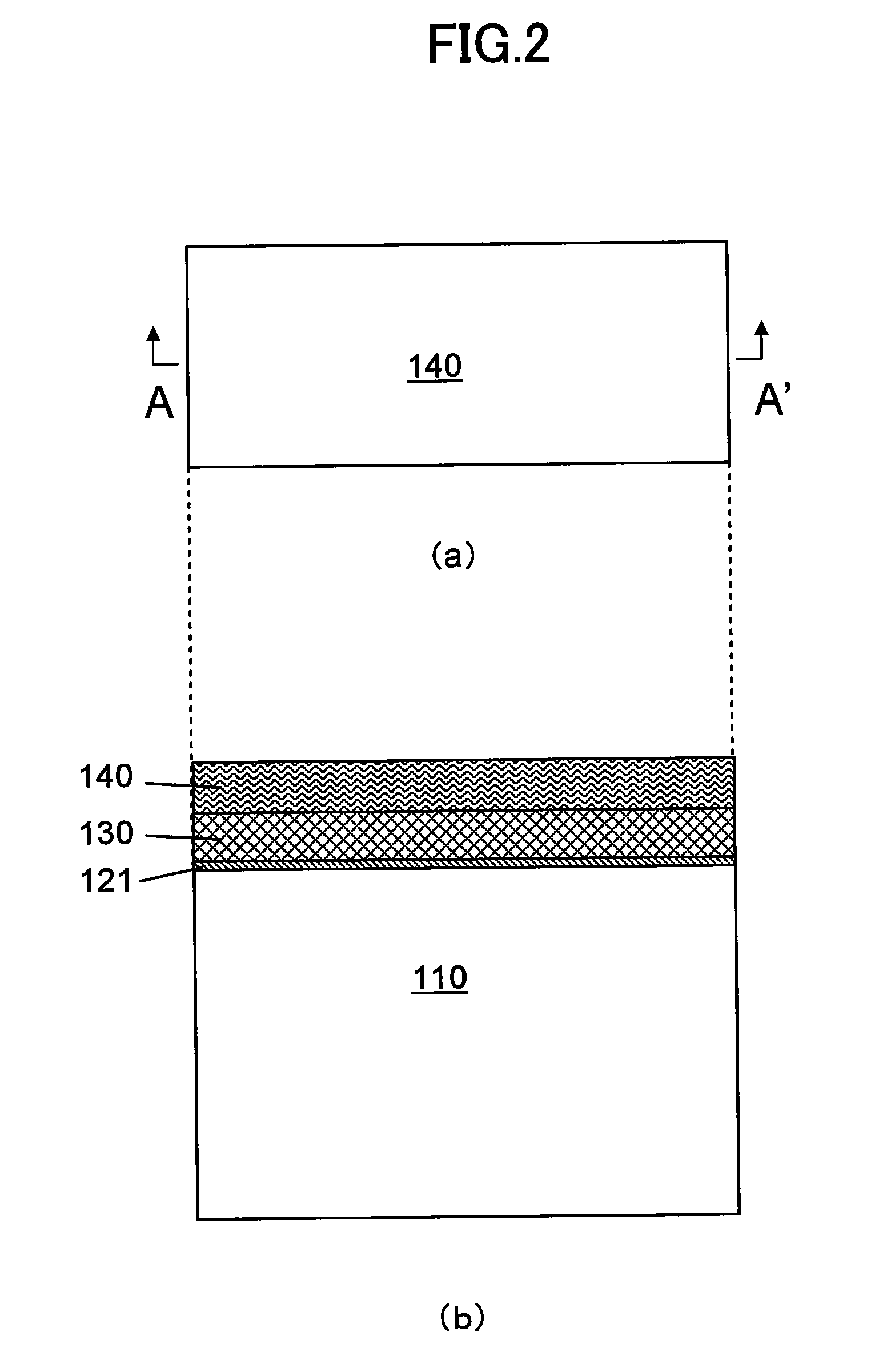
[0149]A first flat silicon layer 112 which is a first flat semiconductor layer, is formed on a silicon substrate 110 which is a substrate, and a first columnar silicon layer 113 which is a first columnar semiconductor layer, is formed on the first flat silicon layer 112. A source diffusion layer 200 which is a first semiconductor layer of a second conductive type, is formed in a lower portion of the first columnar silicon layer 113 and an upper portion (or an entirety) of the flat silicon layer 112, and a drain diffusion layer 201 which is a second semiconductor layer of the second conductive type, is formed in an upper po...


PUM


Abstract

This invention provides a method of manufacturing a semiconductor device, which comprises the steps of: forming a first columnar semiconductor layer on a first flat semiconductor layer; forming a first semiconductor layer of a second conductive type in a lower portion of the first columnar semiconductor layer; forming a first insulating film around a lower sidewall of the first columnar silicon layer; forming a gate insulating film and a gate electrode around the first columnar silicon layer; forming a sidewall-shaped second insulating film to surround an upper sidewall of the first columnar silicon layer; forming a semiconductor layer of a first conductive type between the first semiconductor layer of the second conductive type and a second semiconductor layer of the second conductive type; and forming a metal-semiconductor compound on an upper surface of the first semiconductor layer of the second conductive type.

Description

RELATED APPLICATIONS[0001]Pursuant to 35 U.S.C. § 119(e), this application claims the benefit of the filing date of Provisional U.S. Patent Application Ser. No. 61 / 214,584 filed on Apr. 24, 2009. This application also claims priority under 35 U.S.C. § 119(a) to JP2009-119233 filed on April 20, 2009. The entire contents of these applications are hereby incorporated by reference.BACKGROUND OF THE INVENTION[0002]1. Field of the Invention[0003]The present invention relates to a semiconductor device and a method of manufacturing the semiconductor device.[0004]2. Description of the Related Art[0005]In semiconductor integrated circuits, particularly an integrated circuit using a MOS transistor, the degree of integration has become increasingly higher. Along with such a high degree of integration, miniaturization of a MOS transistor for highly integrated circuits has been progressed into a nano region. The progress in miniaturization of the MOS transistor involves problems about difficulty ...

Claims


Application Information

Patent Timeline
Patent Type & Authority Applications(United States)
IPC IPC(8): H01L29/78H01L21/336
CPCH01L29/42356H01L29/42392H01L29/78642H01L29/66666H01L29/7827H01L29/458
Inventor MASUOKA, FUJIONAKAMURA, HIROKIARAI, SHINTAROKUDO, TOMOHIKOSINGH, NAVABBUDDHARAJU, KAVITHA DEVINANSHENG, SHENSAYANTHAN, RUKMANI DEVI
Owner UNISANTIS ELECTRONICS SINGAPORE PTE LTD
Why Eureka
Try Eureka