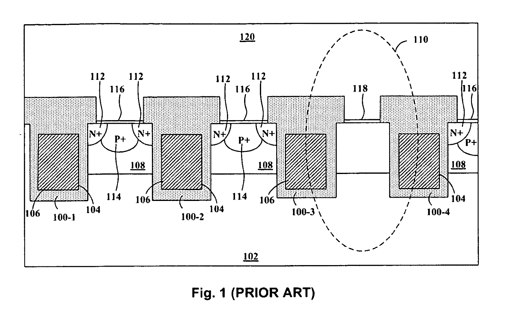
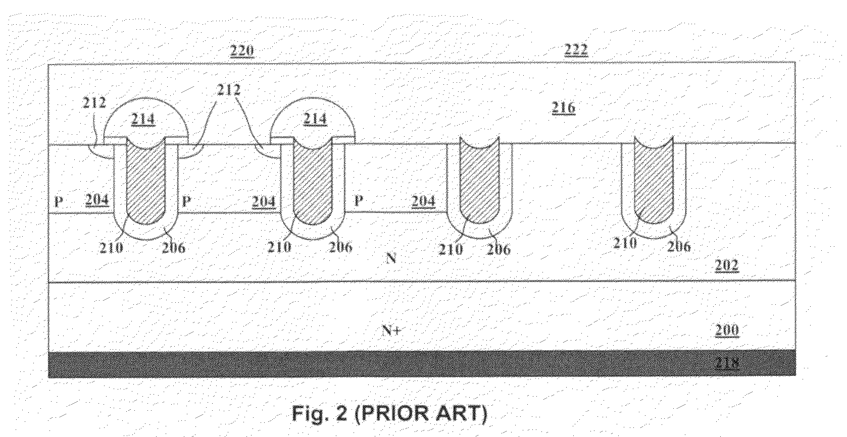
[0013]One
advantage of the present invention is that,
doping regions of a second
semiconductor doping type, e.g., P dopant, marked by p* regions as shown in FIGS. 3 to 6, are formed surrounding the lower portions of
trench gate sidewalls to decouple trench gates from the drain such that the
coupling charges between trench gates and the drain can be reduced. Furthermore,
doping regions of a first
semiconductor doping type, e.g., N dopant, marked by n* regions as shown in FIGS. 3 to 6, are formed right below the trench bottoms to provide a current path between the drain to the source such that the decoupling p* regions will not inadvertently increase the resistance between the drain and source but Crss can be significantly reduced to a value that is about half or even lower when compared with the
capacitance of the conventional devices because the Crss (
Capacitance between gate and drain) or Qgd will be mainly determined by trench width in the present invention when compared with the conventional devices as shown in FIG. 1 and FIG. 2.
[0014]Another
advantage of the present invention is that, the planar contact for both MOSFET devices and Schottky rectifier are replaced by trench contact structure. By employing this trench contact, the devices are able to be shrunk to achieve low specific on-resistance for
trench MOSFET, and, at the same time, achieve low Vf (
forward voltage) and low Ir (
reverse leakage current) for Schottky rectifier.
[0015]Another
advantage of the present invention is that, there's no need to use additional
mask to open the
anode of Schottky rectifier in fabricating process according to this invention, therefore cost saving is achieved.
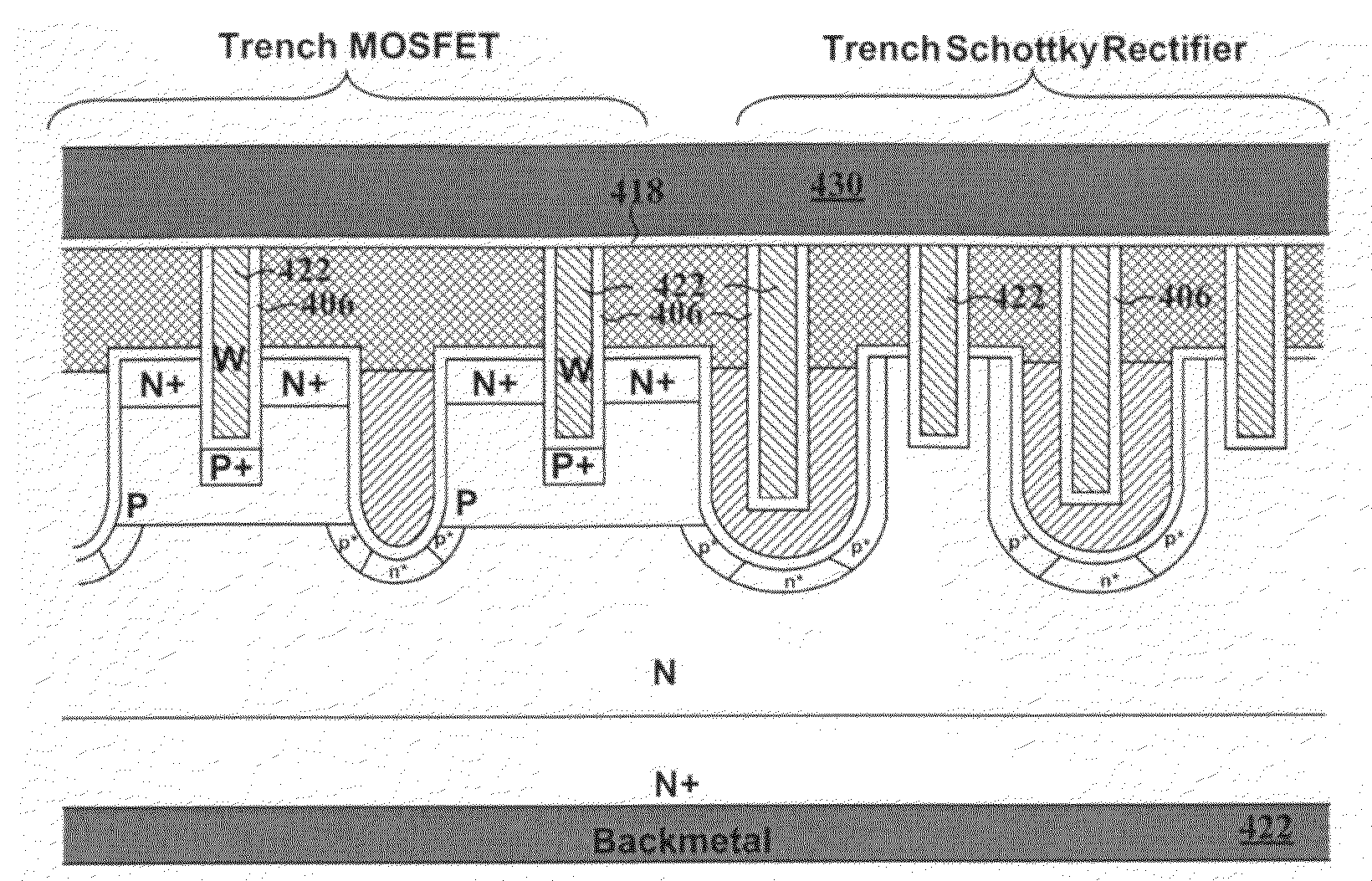
[0016]Briefly, in a preferred embodiment, as shown in FIG. 3, the present invention disclosed an integrated device
cell formed on a heavily doped substrate of a first
semiconductor doping type comprising: a trench MOSFET and a trench Schottky rectifier. Said trench MOSFET further comprises: trench gates filled with doped poly above a layer of
gate oxide and surrounded by a source region of first semiconductor doping type encompassed in a
body region of second semiconductor doping type above a drain region disposed on the bottom surface of said substrate; tilt-angle implanted regions of the opposite dopant type to substrate surrounding the lower portions of trench gates sidewalls to further reduce Qgd; doping regions of the same dopant type as the substrate right below
trench gate bottoms for functioning as a current path between the drain to the source for preventing a resistance increase caused by the doping regions surrounding the lower portions of the trench gates sidewalls; trench contacts penetrating a thick
oxide layer and filled with
tungsten plugs padded with
barrier layer of Ti /
TiN or Co /
TiN to connect all the source regions to source
metal of Al alloys or
Copper deposited onto a resistance-reduction layer of Ti or Ti /
TiN; P+ regions at the bottom of each contact trench to further reduce
contact resistance;. The trench Schottky rectifier further comprises: trench gates filled with doped poly and penetrating into epitaxial layer built on said substrate; tilt-angle doping regions of the opposite dopant type to the substrate surrounding the sidewalls of trench gates; doping regions of the same dopant type as the substrate right below
trench gate bottoms; contact trenches with a layer of Ti / TiN or Co / TiN lining the inner surface; P+regions at the bottom of each contact trench except trenches penetrating into trench gates introduced in the same step with those of trench MOSFET;
tungsten plug filled into each the contact trench as
anode material for trench Schottky and connected to
metal layer of Al alloys or
Copper which is the same
metal layer as source metal for trench MOSFET. What should be noticed is that, according to this preferred embodiment, the integrated structure has single
gate oxide and the trench gates in Schottky rectifier is not connected with trench gates in trench MOSFET but shorted with anode of Schottky rectifier.
[0017]Briefly, in another preferred embodiment, as shown in FIG. 4, the structure disclosed is similar to that shown in FIG. 3 except that, there is no P+ region underneath each contact trench in trench Schottky rectifier by using additional P+ mask to block P+
Ion Implantation during fabricating process. [00016] Briefly, in another embodiment, the present invention disclosed an integrated structure formed on a heavily doped substrate of a first semiconductor doping type comprising a trench MOSFET and a trench Schottky rectifier and in parallel with a trench gate portion. Said trench MOSFET further comprises: trench gates filled with doped poly above a layer of
gate oxide and surrounded by a source region of the first semiconductor doping type encompassed in a
body region of the second semiconductor doping type above a drain region disposed on bottom surface of said substrate; tilt-angle implanted regions of the opposite dopant type to substrate surrounding the lower portions of trench gate sidewalls to further reduce Qgd; doping regions of the same dopant type as the substrate right below trench gate bottoms for functioning as a current path between the drain to the source for preventing a resistance increase caused by the doping regions surrounding the lower portions of the trench gates sidewalls; trench contacts penetrating a thick
oxide layer and filled with
tungsten plugs padded with layer of Ti / TiN or Co / TiN to connect all the source regions to source metal of Al alloys or
Copper deposited onto a resistance-reduction layer of Ti or Ti / TiN; P+ regions at the bottom of each contact trench to further reduce
contact resistance. The trench Schottky rectifier further comprises: trench gates filled with doped poly and penetrating epitaxial layer built on said substrate; doping regions of the opposite dopant type to the substrate surrounding the sidewalls of trench gates; doping regions of the same dopant type as the substrate right below trench gate bottoms; contact trenches with a layer of Ti / TiN or Co / TiN lining the inner surface; P+ regions at the bottom of each contact trench introduced in the same step as those of trench MOSFET; tungsten plug filled into each the contact trench as anode material for trench Schottky and connected to metal layer of Al alloys or Copper which is the same metal layer as source metal for trench MOSFET. What should be noticed is that, according to this preferred embodiment, the trench gate in Schottky rectifier introduced in not shorted with anode via trench contact like the first embodiment, and trench MOSFET and trench Schottky rectifier have common trench gate.
[0018]Briefly, in another preferred embodiment, as shown in FIG. 6, the structure disclosed is similar to that shown in FIG. 5 except that, there is no P+ region underneath each contact trench in trench Schottky rectifier by using additional P+ mask to block P+
Ion Implantation during fabricating process.

