
Photovoltaic device and process for producing same

a photovoltaic device and photovoltaic technology, applied in the direction of semiconductor/solid-state device manufacturing, semiconductor devices, electrical devices, etc., can solve the problems of fine uneven texture on the substrate-side surface of the metal layer, insufficient modification of the layer structure alone, and increase in crystal grain size, so as to reduce the height variation of surface unevenness, improve the effect of surface plasmon absorption, and reduce the effect of uneven heigh

Inactive Publication Date: 2010-10-28
MITSUBISHI HEAVY IND LTD
View PDF6 Cites 13 Cited by
  • Summary
  • Abstract
  • Description
  • Claims
  • Application Information

AI Technical Summary

Benefits of technology

[0008]In order to enhance the conductivity, the transparent electrode layer is generally deposited under conditions including a high substrate temperature, for example a substrate temperature within a range from 120 to 200° C. By conducting the deposition under high-temperature conditions, the size of the crystal grains increases, enabling the conductivity of the transparent electrode layer to be increased as a result of improved film quality and a reduction in the quantity of crystal grain boundaries. However, because the deposition is conducted under conditions including a high substrate temperature, crystallization progresses significantly, causing an increase in the crystal grain size. As the crystal grain size increases, the surface shape of the transparent electrode layer reflects the shape of the crystal grains, and develops a fine uneven texture. In other words, a problem arises in that a fine uneven texture is formed on the substrate-side surface of the metal layer.
[0029]By forming the second transparent electrode layer at a substrate temperature of not less than 20° C. and not more than 90° C., a photovoltaic device can be produced in which the back electrode layer-side surface of the second transparent electrode layer has the shape described above. The surface shape of the second transparent electrode layer is optimized so as to reduce light loss due to surface plasmon absorption at the back electrode layer and increase the quantity of reflected light. As a result, a photovoltaic device having superior output and conversion efficiency can be obtained.

Problems solved by technology

However, in order to achieve further improvements in the conversion efficiency, modification of the layer structure alone is inadequate.
However, because the deposition is conducted under conditions including a high substrate temperature, crystallization progresses significantly, causing an increase in the crystal grain size.
In other words, a problem arises in that a fine uneven texture is formed on the substrate-side surface of the metal layer.

Method used


Image

  • Photovoltaic device and process for producing same
  • Photovoltaic device and process for producing same
  • Photovoltaic device and process for producing same

Examples


examples

(Effect of Substrate Temperature During Deposition on the Surface Shape of a GZO Film Surface)

[0092]A GZO film was deposited on a glass substrate. Using a DC sputtering apparatus with a Ga-doped ZnO sintered body as the target, film deposition was conducted under conditions including a discharge gas composed of argon and oxygen, a film thickness target of 80 nm, and a substrate temperature of 25° C., 60° C., 135° C. or 200° C.

[0093]The surface shapes of the GZO films deposited at each of the different substrate temperatures were inspected using an AFM (NanoScope D-3100, manufactured by Digital Instruments Inc.), with each sample inspected using a tapping mode within two arbitrary fields of view, under conditions including a field of view of 2 μm×2 μm, a resolution of 512 pixels, and a Z-range of either 100 nm / div or 500 nm / div. An average value for the surface area magnification ratio was determined from the obtained AFM images. Using a cross-sectional profile of the AFM image, the ...


PUM


Abstract

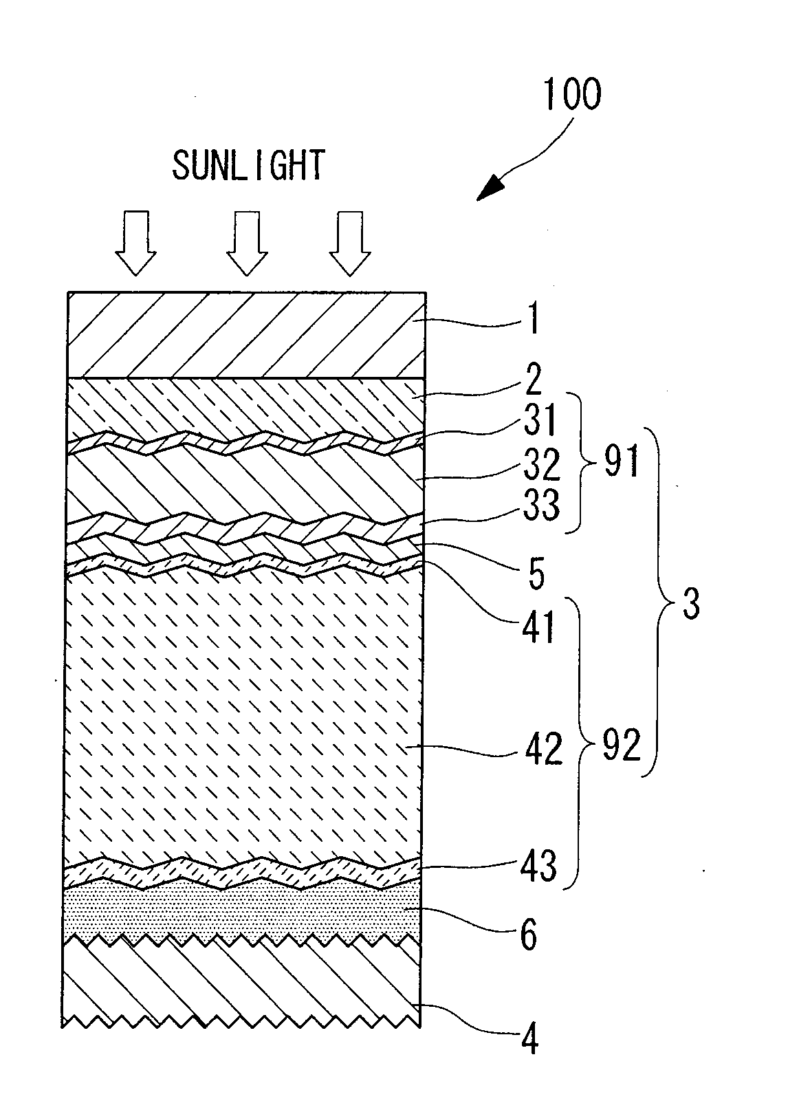
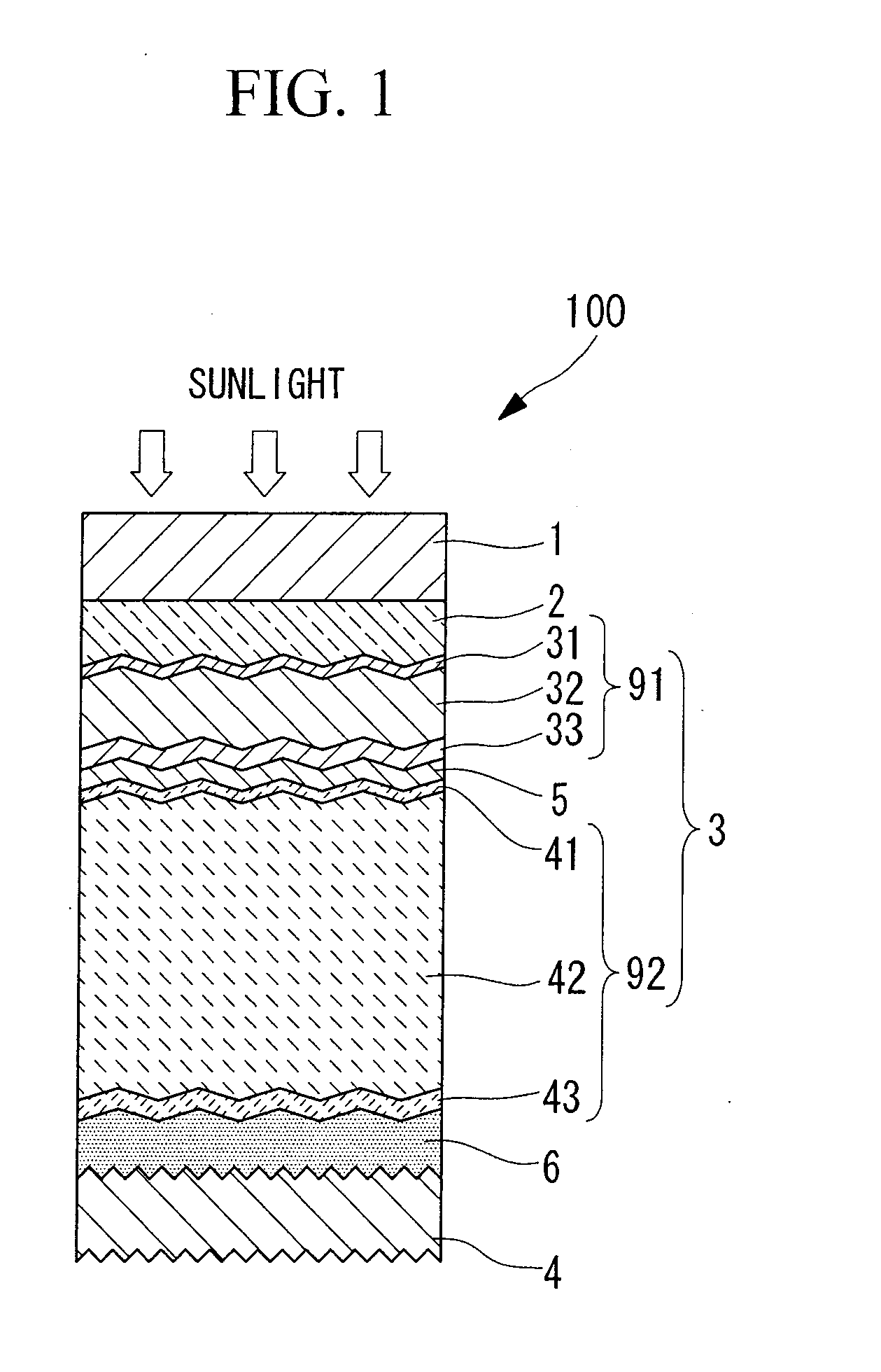
A photovoltaic device that exhibits improved light absorption properties for the electric power generation layer and a process for producing such a photovoltaic device are provided by optimizing the surface shape of the back surface structure. A photovoltaic device 100 comprising a first transparent electrode layer 2, an electric power generation layer 3, a second transparent electrode layer 6 and a back electrode layer 4 provided sequentially on a substrate 1, wherein the back electrode layer 4 comprises a thin film of silver, and the surface of the second transparent electrode layer 6 on the surface of the back electrode layer 4 has a fine uneven texture, for which the surface area magnification ratio relative to the projected surface area is not less than 10% and not more than 32%. Also, a photovoltaic device comprising a first transparent electrode layer 2, an electric power generation layer 3, a second transparent electrode layer 6 and a back electrode layer 4 provided sequentially on a substrate 1, wherein the back electrode layer 4 comprises a thin film of silver, the back electrode layer-side surface of the second transparent electrode layer 6 has a fine uneven texture, and the second transparent electrode layer 6 comprises needle-like crystals.

Description

TECHNICAL FIELD[0001]The present invention relates to a photovoltaic device and a process for producing the same, and relates particularly to a solar cell that uses silicon as the electric power generation layer.BACKGROUND ART[0002]The use of solar cells as photovoltaic devices that receive light and convert the energy into electrical power is already known. Amongst solar cells, thin-film type solar cells in which thin films of silicon-based layers are stacked together to form an electric power generation layer (photovoltaic layer) offer various advantages, including the comparative ease with which the surface area can be increased, and the fact that the film thickness is approximately 1 / 100th that of a crystalline solar cell, meaning minimal material is required. As a result, thin-film silicon-based solar cells can be produced at lower cost than crystalline solar cells. However, a drawback of thin-film silicon-based solar cells is the fact that the conversion efficiency is lower th...

Claims


Application Information

Patent Timeline
IPC IPC(8): H01L31/0352H01L31/18H01L31/0224
CPCH01L31/022425H01L31/0236H01L31/076H01L31/056Y02E10/548Y02E10/52H01L31/046H01L31/1884H01L31/02366H01L31/0463
Inventor SAKAI, SATOSHIASAHARA, YUJIKOBAYASHI, YASUYUKIMORI, MASAFUMITSURUGA, SHIGENORIYAMASHITA, NOBUKI
Owner MITSUBISHI HEAVY IND LTD
Learn More