Method for preparing substrate with periodical structure

a technology of periodical structure and substrate, applied in the field of periodical structure preparation, can solve the problems of high manufacturing cost, low production capacity, high energy engraving process, etc., and achieve the effects of reducing the probability of substrate damage, uniform periodical structure, and simple and inexpensive way

Inactive Publication Date: 2010-10-28
AUROTEK CORP
View PDF5 Cites 13 Cited by
  • Summary
  • Abstract
  • Description
  • Claims
  • Application Information

AI Technical Summary

Benefits of technology

[0023]According to the method of the present invention, the nano-sized balls can serve as a template for forming an etching template. Hence, the photolithography process can be replaced by the process of forming the nano-sized ball layer. At the same time, the wet etching process is used in the present invention to etch the substrate, so it is possible to reduce the probability of damaging the substrate and obtain a substrate with a uniform periodical structure. Therefore, by using the method of the present invention, the substrate can be patterned to form the periodical structure thereon in a simple, inexpensive, and rapid way.

Problems solved by technology

However, high-energy engraving process has disadvantages of high manufacturing cost and low production capacity.
Although nano-imprinting technology has lower manufacturing cost and higher production capacity than high-energy engraving process, it still cannot meet the requirements for low manufacturing cost and high production capacity.
Although the method of dry etching can produce a substrate having a periodical structure with uniform and regular micro-cavities, there are still some disadvantages with the aforementioned process.
First, the manufacturing cost of photolithography is high and the production rate is low.
However, the photo-mask with sub-micro size is very expensive, and the manufacturing cost of the photo-mask is even more expensive when a periodical structure with a size of 500 nm or less is desired.
In addition, the RIE machine is expensive, the RIE process is slow, and the substrate is damaged easily when the RIE process is used.
The wet etching process can protect the substrate from damage and the surface of the patterned substrate is a natural lattice plane, but the uniformity of the periodical structure is not good enough if the parameter of the wet etching process is not controlled properly.
In addition, the photolithography is still performed in the aforementioned process, so the problems of high manufacturing cost and low production rate still exist.

Method used


Image

  • Method for preparing substrate with periodical structure
  • Method for preparing substrate with periodical structure
  • Method for preparing substrate with periodical structure

Examples


Embodiment Construction

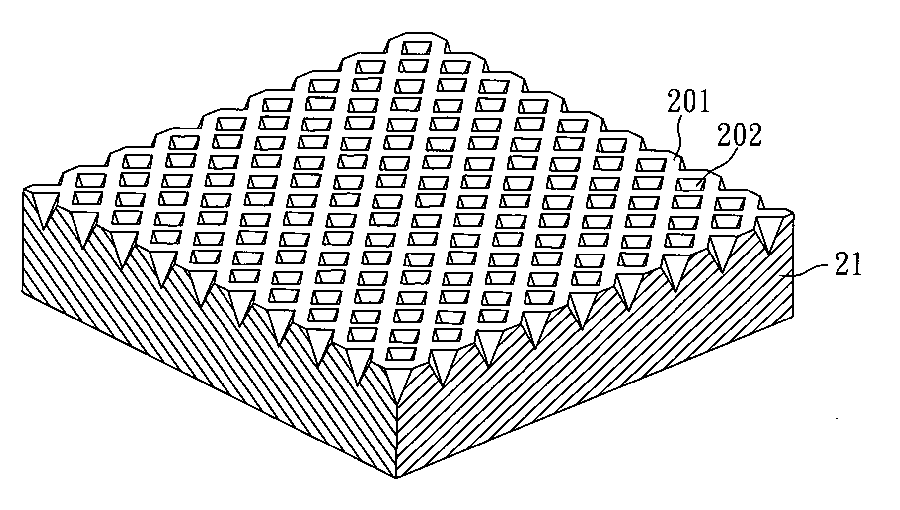
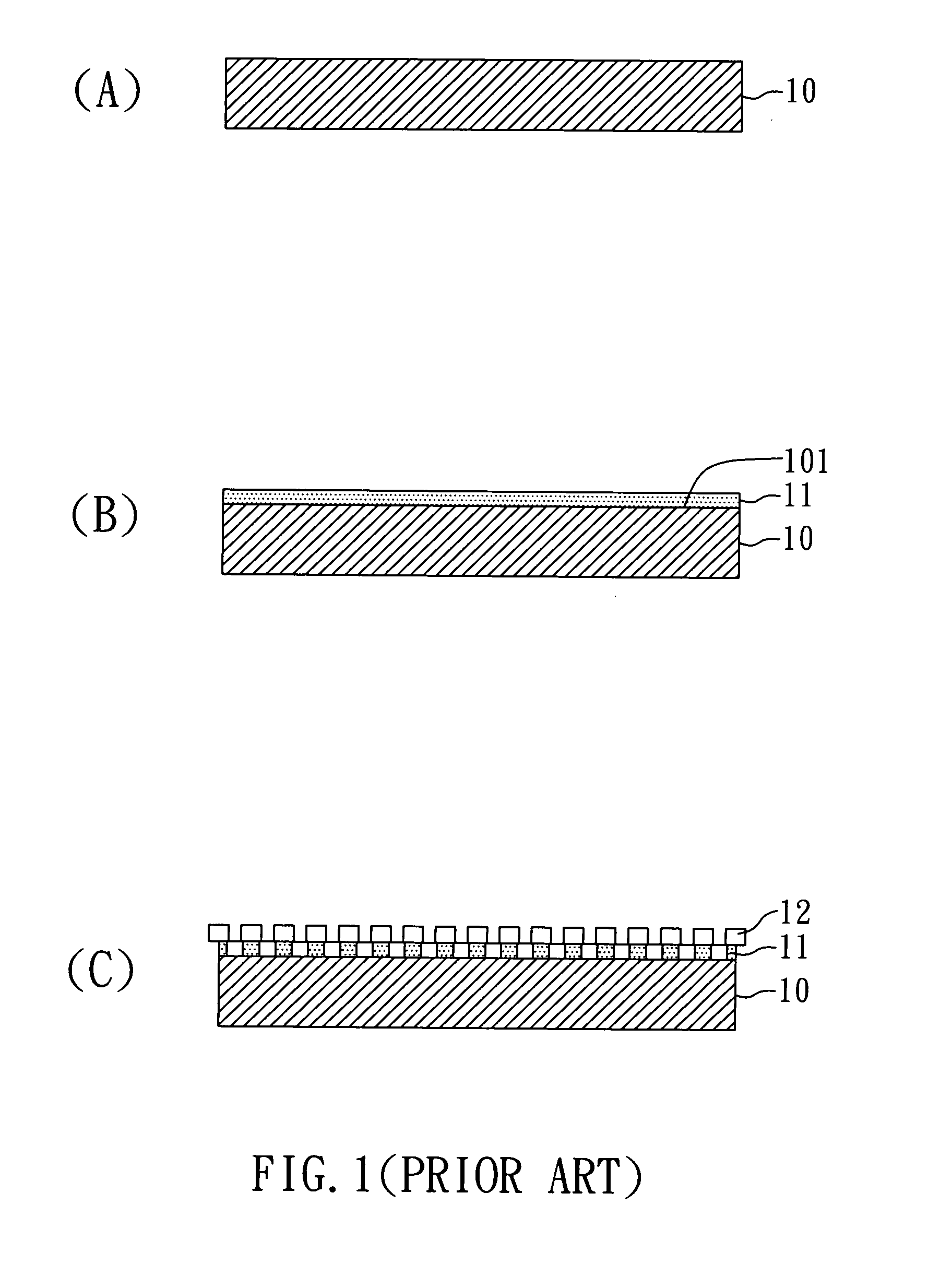
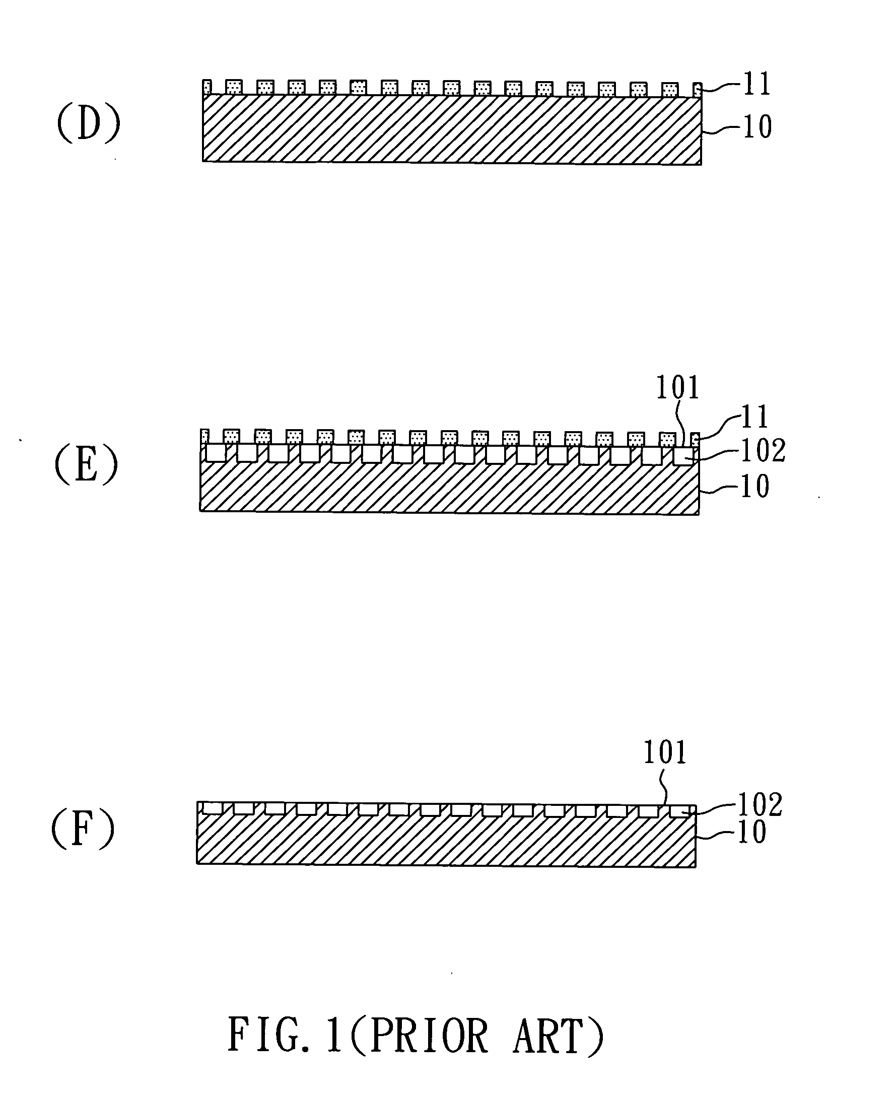
[0032]FIGS. 3A to 3F are cross-sectional views illustrating a process that nano-sized balls are arranged on a surface of a substrate in a preferred embodiment of the present invention. First, as shown in FIG. 3A, a substrate 21 is provided, and a colloid solution 25 is provided in a container 26, wherein the colloid solution 25 comprises plural nano-sized balls (not shown in the figure) and a surfactant (not shown in the figure). Next, the substrate 21 is placed in the container 26, and the substrate 21 is immersed in the colloid solution 25 entirely, as shown in FIG. 3B. After several minutes, the nano-sized balls 22 are arranged on the surface of the substrate 21 orderly to form a “nano-sized ball layer”, as shown in FIG. 3C. Then, a volatile solution 27 is added into the container 26 to evaporate the colloid solution 25, as shown in FIG. 3D. Finally, after the colloid solution 25 is evaporated completely, as shown in FIG. 3E, the substrate 21 is taken out from the container 26, a...


PUM

PropertyMeasurementUnit
diametersaaaaaaaaaa
sizeaaaaaaaaaa
lengthaaaaaaaaaa

Abstract

A method for preparing a substrate with periodical structure, comprising the following steps: (A) providing a substrate and plural nano-sized balls, wherein the nano-sized balls are arranged on the surface of the substrate; (B) depositing a cladding layer on partial surface of the substrate and the gaps between the nano-sized balls; (C) removing the nano-sized balls; (D) etching the substrate by using the cladding layer as a mask; and (E) removing the mask to form a periodical structure on the surface of the substrate. In the present invention, the nano-sized balls are used as a template for forming the mask. Hence, compared with the lithography, when the method of the present invention is used to prepare a substrate with a periodical structure, the duration of the process and the manufacturing cost can be decreased.

Description

BACKGROUND OF THE INVENTION[0001]1. Field of the Invention[0002]The present invention relates to a method for preparing a substrate with a periodical structure and, more particularly, to a method, which can prepare a substrate with a periodical structure in a rapid and inexpensive way and protect the substrate from damage.[0003]2. Description of Related Art[0004]A photonic crystal is a periodical structure, which can control and manipulate the flow of light having a certain frequency range, and also can prevent the propagation of light having other frequency ranges. The photonic crystals work at optical wavelengths, so the photonic crystals have to be formed of a periodic sub-micro sized or nano sized structure. Currently, the photonic crystals can be applied widely in the fields of optical communications and optical calculators, and also applied to photoelectric devices to improve the efficiency thereof.[0005]The photonic crystals are generally manufactured by patterning a substrat...

Claims


Application Information

Patent Timeline
Patent Type & Authority Applications(United States)
IPC IPC(8): C23F1/00
CPCB82Y20/00G02B1/005H01L2933/0083H01L31/0352H01L31/035281G02B1/105
Inventor LI, CHUNG-HUALEE, SHENG-RU
Owner AUROTEK CORP
Why Eureka
Try Eureka