Semiconductor device

a technology of semiconductors and semiconductors, applied in the field of semiconductor devices, can solve the problems of dispersion of wiring resistance, defective resolution of photolithography, and various inconveniences, and achieve the effect of preventing dishing

Active Publication Date: 2010-10-28
ROHM CO LTD
View PDF6 Cites 16 Cited by
  • Summary
  • Abstract
  • Description
  • Claims
  • Application Information

AI Technical Summary

Benefits of technology

[0016]An object of the present invention is to provide a semiconductor device capable of preventing dishing resulting from CMP treatment.

Problems solved by technology

This may result in various inconveniences such as dispersion in wiring resistance, defective resolution in photolithography and a short circuit between the respective wires.
Such inconveniences cause reduction of the yield in the manufacturing steps and reduction of the reliability in quality of the semiconductor device.
This may result in various inconveniences such as defective resolution in photolithography and a short circuit between the respective wiring layers.

Method used


Image

  • Semiconductor device
  • Semiconductor device
  • Semiconductor device

Examples


first embodiment

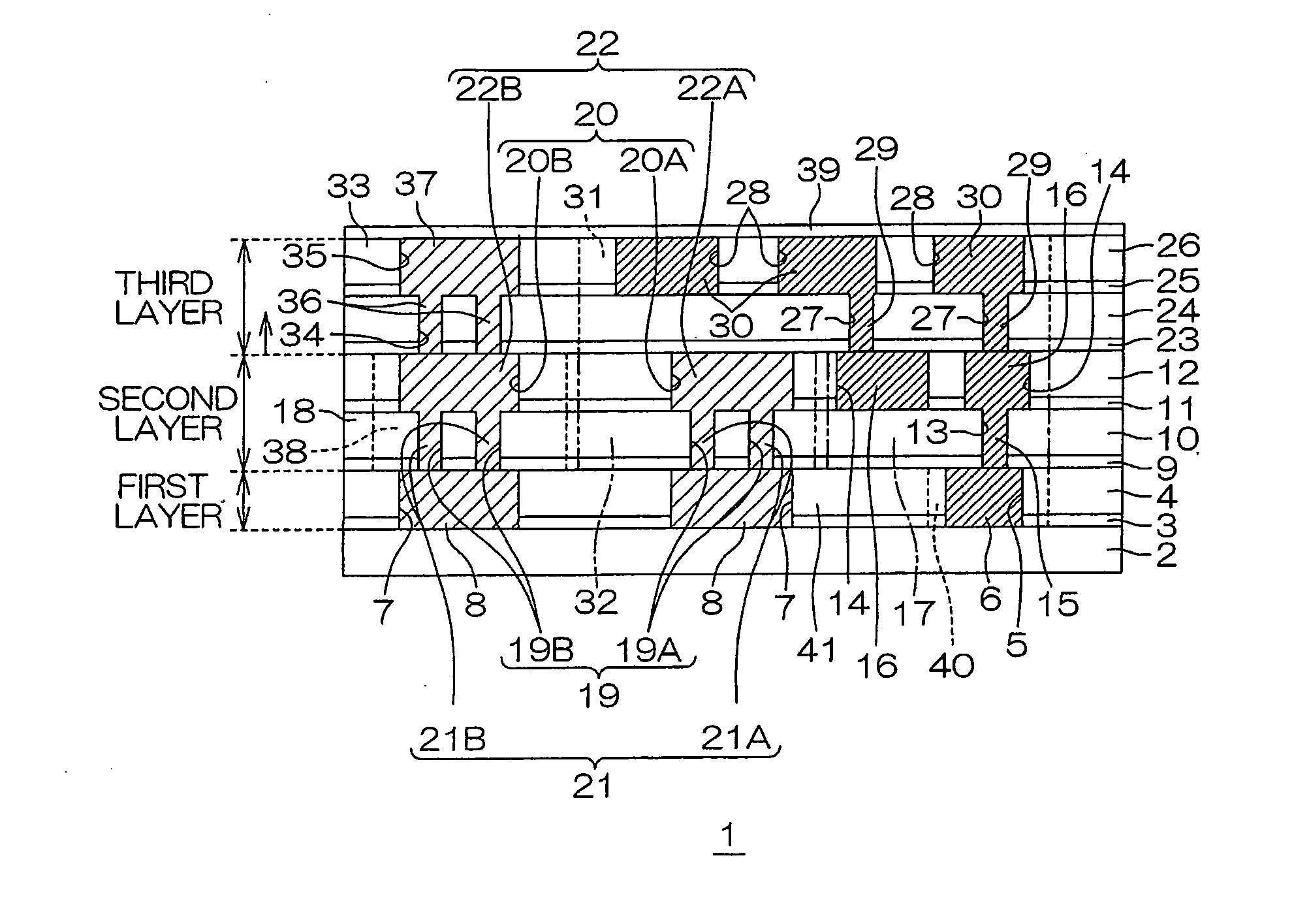
[0039]FIG. 1 is a schematic sectional view showing the structure of a semiconductor device according to the present invention.

[0040]The semiconductor device 1 has a multilevel interconnection structure including a semiconductor substrate 2 and first, second and third layers formed by laminating these layers on the semiconductor substrate 2 in this order.

[0041]The semiconductor substrate 2 is made of a semiconductor material such as silicon (Si), for example, and a semiconductor element and the like are formed on the surface layer thereof.

[0042]The first layer is formed on the semiconductor substrate 2. More specifically, a diffusion preventing layer 3 and an interlayer film 4 are laminated on the semiconductor substrate 2 in this order, thereby forming the first layer.

[0043]The diffusion preventing film 3 is formed of silicon carbide (SiC), for example.

[0044]The interlayer film 4 is formed using an insulating material having a relatively low dielectric constant. For example, SiOC (d...

second embodiment

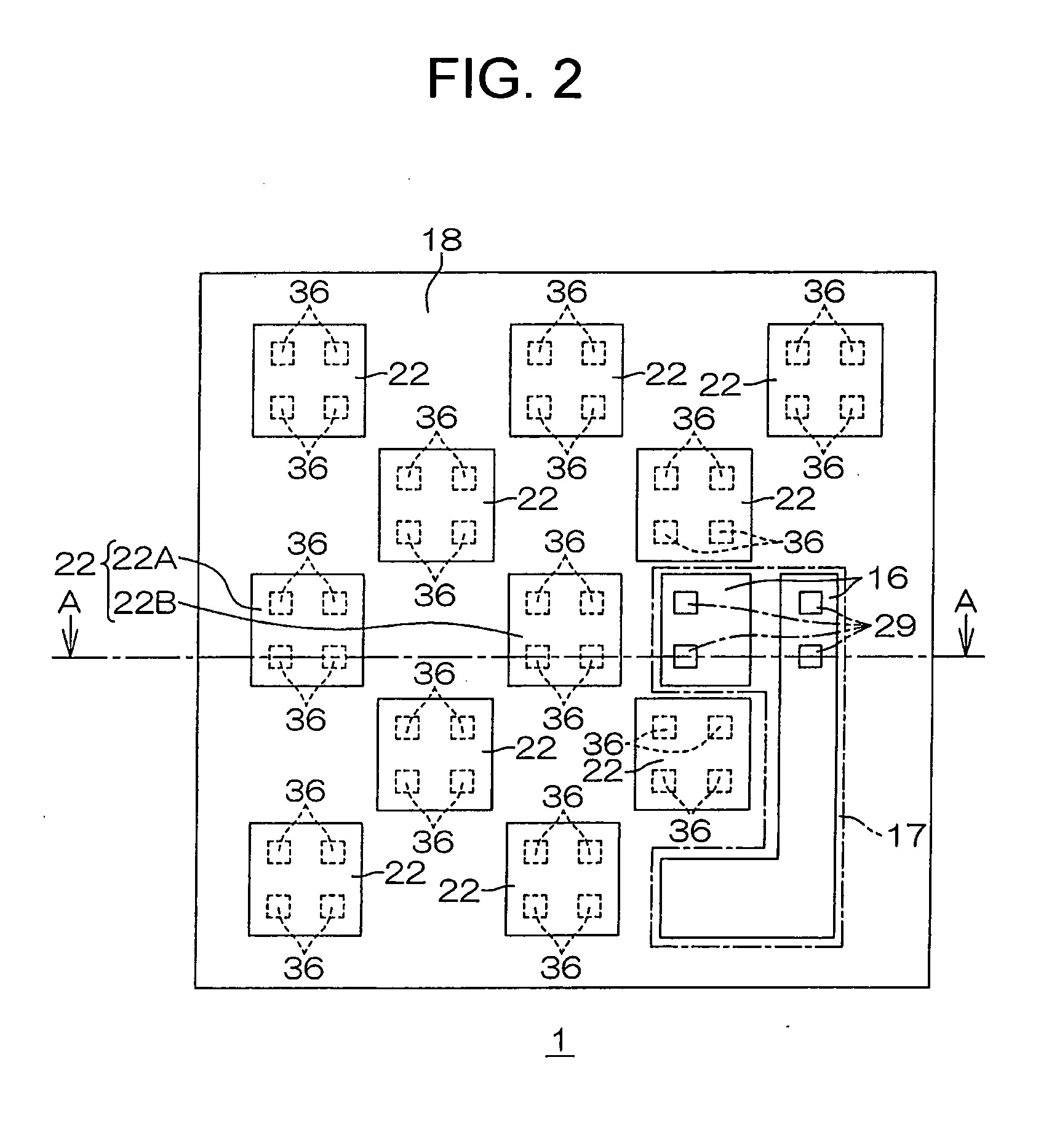
[0099]FIG. 3 is a schematic plan view showing the structure of a semiconductor device according to the present invention.

[0100]Referring to FIG. 3, the semiconductor device 51 is generally rectangularly formed in plan view, for example.

[0101]A plurality of bonding pads 52 (12 in this embodiment, for example) are arranged on the upper surface (surface) 51A of the semiconductor device 51 along the periphery of the upper surface 51A at intervals from one another. Each bonding pad 52 is made of a metallic material such as copper, aluminum or an aluminum-copper alloy, for example, and generally rectangularly formed in plan view.

[0102]FIG. 4 is a plan view showing the circumference of each bonding pad 52 shown in FIG. 3. FIG. 5 is a sectional view taken along the line B-B in FIG. 4.

[0103]The semiconductor device 51 includes a semiconductor substrate 53 as well as a first wiring layer 54, a second wiring layer 55, a third wiring layer 56, a fourth wiring layer 57 and a pad layer 58 success...


PUM

PropertyMeasurementUnit
dielectric constantaaaaaaaaaa
metallicaaaaaaaaaa
insulatingaaaaaaaaaa

Abstract

The semiconductor device according to the present invention includes a semiconductor substrate, a first insulating layer laminated on the semiconductor substrate, a first metal wiring pattern embedded in a wire-forming region of the first insulating layer, a second insulating layer laminated on the first insulating layer, a second metal wiring pattern embedded in a wire-forming region of the second insulating layer and first dummy metal patterns embedded each in a wire-opposed region opposing to the wire-forming region of the second insulating layer and in a non-wire-opposed region opposing to a non-wire-forming region other than the wire-forming region of the second insulating layer, the wire-opposed region and the non-wire-opposed region each in a non-wire-forming region other than the wire-forming region of the first insulating layer.

Description

CROSS-REFERENCE TO RELATED APPLICATIONS[0001]This application is a divisional of U.S. application Ser. No. 11 / 979,728, filed Nov. 7, 2007. Further, this application claims the benefit of priority of Japanese applications serial number 2006-302982, filed Nov. 8, 2006 and serial number 2006-306998, filed Nov. 13, 2006. The disclosures of these prior U.S. and Japanese applications are incorporated herein by reference.BACKGROUND OF THE INVENTION[0002]1. Field of the Invention[0003]The present invention relates to a semiconductor device, and more specifically, it relates to a semiconductor device having damascene wires.[0004]2. Description of Related Art[0005]With the recent integration of a semiconductor device, refinement of wires is required. In order to satisfy this requirement, employment of copper (Cu) wires or the like having small electrical resistance in place of conventional aluminum (Al) wires or the like is studied.[0006]The damascene process is known as a method of forming f...

Claims


Application Information

Patent Timeline
Patent Type & Authority Applications(United States)
IPC IPC(8): H01L29/40
CPCH01L21/7684H01L21/76895B23D51/125H01L23/528H01L24/05H01L23/5226H01L23/522H01L2924/01079H01L23/481H01L23/5222H01L2924/01078H01L2924/01029H01L23/5329H01L2924/01013H01L21/76802H01L21/76877H01L23/53228
Inventor NAKAO, YUICHIKAGEYAMA, SATOSHINAITOU, MASARU
Owner ROHM CO LTD
Why Eureka
Try Eureka