At-Speed Scan Testing With Controlled Switching Activity

a scanning activity and control technology, applied in the field of integrated circuit scanning, can solve the problems of high switching activity at circuit nodes during the test, high ir (product of current and resistance) drop, and cut to operate in non-functional states during the tes

Active Publication Date: 2010-10-28
SIEMENS PROD LIFECYCLE MANAGEMENT SOFTWARE INC
View PDF14 Cites 16 Cited by
  • Summary
  • Abstract
  • Description
  • Claims
  • Application Information

AI Technical Summary

Benefits of technology

[0015]Aspects of the invention relate to techniques of at-speed scan testing that control the switching activity of a circuit under test so that it is near or at the switching activity of a steady state. With various implementations of the invention, functional background data are used to filled unspecified bits of a test cube to generate a test pattern. Here, functional background data refer to scan cell values observed when the switching activity of a circuit is near or at a steady state. Functional background data can be generated by applying another test pattern for a ...

Problems solved by technology

Functional tests may be used as at-speed tests, but they are expensive due to the cost of generating the tests and the cost of high speed functional testers.
While scan tests are less costly to implement with high fault coverage, they may violate various functional constraints on the circuit under test (CUT) and cause the CUT to operate in non-functional states during a test.
Non-functional characteristics of test stimuli and test responses in scan tests may cause high switching activity at circuit nodes during a test.
High switching activity may cause two problems.
The first problem is overtesting.
High switching activity requires high peak supply currents and thus results in high IR (product of current and resistance) drops.
High IR drops may increase signal propagation delays that would not happen in a functional state of a CUT.
As such, some good IC chips may fail at-speed tests, causing false yield losses.
The second problem is high power dissipation.
High switching activity may cause hot spots and perm...

Method used


Image

  • At-Speed Scan Testing With Controlled Switching Activity
  • At-Speed Scan Testing With Controlled Switching Activity
  • At-Speed Scan Testing With Controlled Switching Activity

Examples


Embodiment Construction

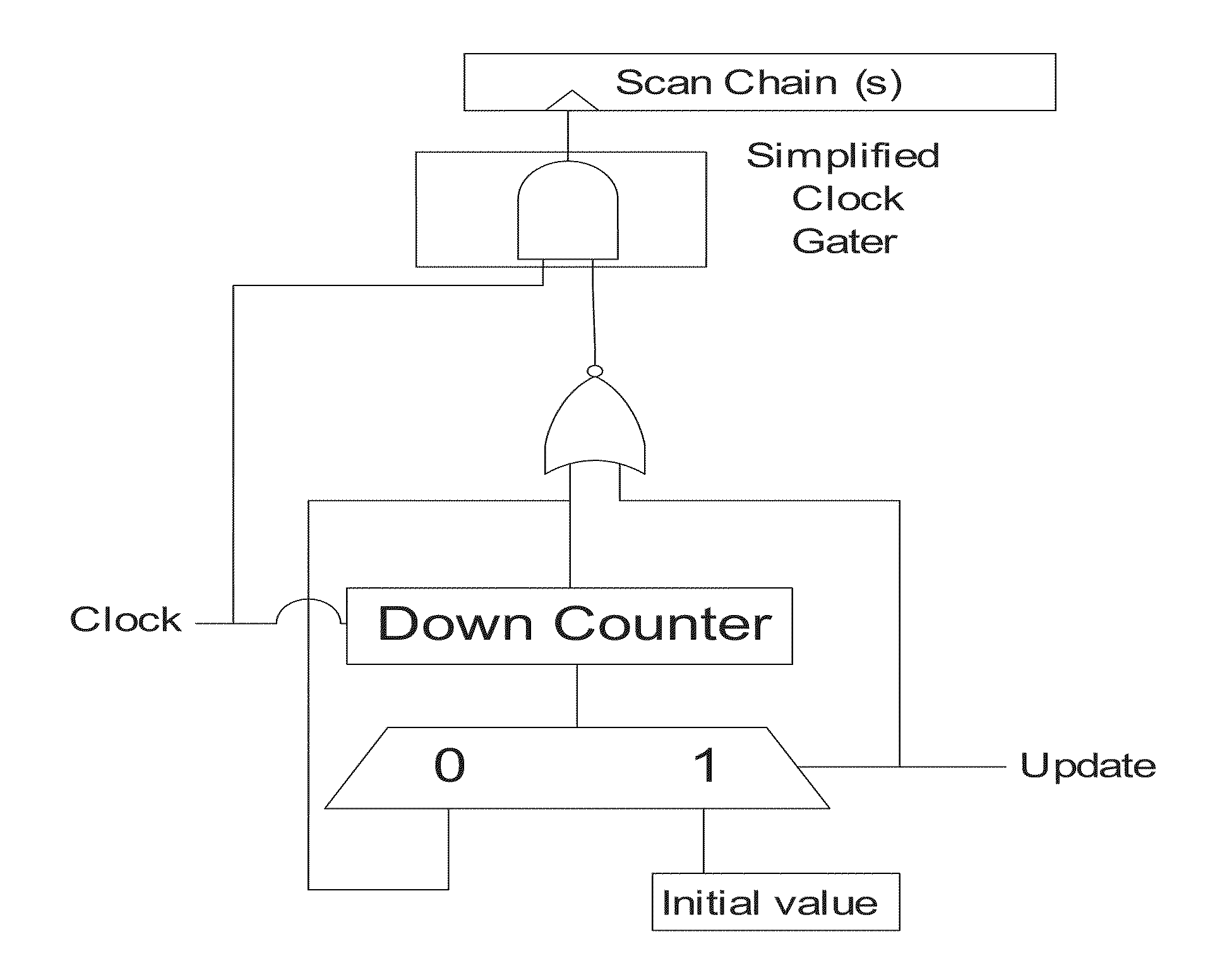
[0029]Various aspects of the present invention relate to techniques of filling unspecified bits of a test cube with functional background data. In the following description, numerous details are set forth for purpose of explanation. However, one of ordinary skill in the art will realize that the invention may be practiced without the use of these specific details. In other instances, well-known features have not been described in details to avoid obscuring the present invention.

[0030]Some of the techniques described herein can be implemented in software instructions stored on a computer-readable medium, software instructions executed on a computer, or some combination of both. Some of the disclosed techniques, for example, can be implemented as part of an electronic design automation (EDA) tool. Such methods can be executed on a single computer or a networked computer.

[0031]Although the operations of the disclosed methods are described in a particular sequential order for convenient...


PUM


Abstract

Test patterns for at-speed scan tests are generated by filling unspecified bits of test cubes with functional background data. Functional background data are scan cell values observed when switching activity of the circuit under test is near a steady state. Hardware implementations in EDT (embedded deterministic test) environment are also disclosed.

Description

RELATED APPLICATIONS[0001]This application claims priority to U.S. Provisional Patent Application No. 61 / 171,777, entitled “A New Method To Reduce Overtesting In Scan Based Design,” filed on Apr. 22, 2009, and naming Janusz Raj ski et al. as inventors, which application is incorporated entirely herein by reference.FIELD OF THE INVENTION[0002]The present invention is directed to scan-based tests of integrated circuits. Various aspects of the invention may be particularly useful for at-speed scan tests.BACKGROUND OF THE INVENTION[0003]At-speed tests, which capture a test response at the rated clock speed, have become more and more important as integrated circuits' feature sizes continue to shrink and operating frequencies continue to increase. Functional tests may be used as at-speed tests, but they are expensive due to the cost of generating the tests and the cost of high speed functional testers. Thus, relatively inexpensive scan-based tests (scan tests) are widely adopted for at-sp...

Claims


Application Information

Patent Timeline
IPC IPC(8): G01R31/3177G06F11/25
CPCG01R31/318575G01R31/318547
Inventor RAJSKI, JANUSZMOGHADDAM, ELHAM K.MUKHERJEE, NILANJANKASSAB, MARK A.LIN, XIJIANG
Owner SIEMENS PROD LIFECYCLE MANAGEMENT SOFTWARE INC
Why Eureka
Try Eureka