Oscillator, oscillator array and an electronic apparatus
an oscillator array and oscillator technology, applied in the direction of oscillator generators, piezoelectric/electrostrictive/magnetostrictive devices, piezoelectric/electrostrictive/magnetostriction machines, etc., can solve the problem of inability to detect substances, difficult manufacturing and handling of such devices, weak mechanical strength, etc. problem, to achieve the effect of high detection sensitivity
- Summary
- Abstract
- Description
- Claims
- Application Information
AI Technical Summary
Benefits of technology
Problems solved by technology
Method used
Image
Examples
embodiment 1
(1) Embodiment 1
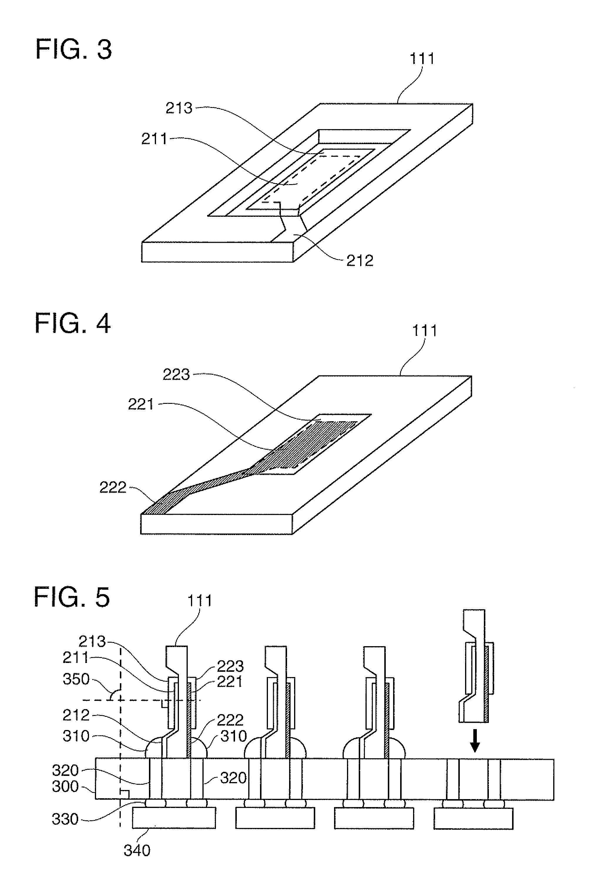
[0084]FIG. 5 is a schematic side view showing a first placement example of vibrators on a substrate in accordance with an embodiment 1. As shown in FIG. 5, a substrate 300 is structured to have a plurality of crystal vibrators 111 erected thereon. The substrate 300 is structured with a first connection section 310, a pass-through wiring 320 and a second connection section 330. Further, an integrated circuit 340 is arranged in the back surface of the substrate 300.
[0085]The pair of excitation electrodes 211 and 221 of the crystal vibrator 111 is connected to the pass-through wiring 320 in the substrate 300 via the pair of lead-out electrodes 212 and 222, respectively, and the first connection section 310. The first connection section 310 is arranged on the front surface of the substrate 300, and connects the crystal vibrator 111 with the pass-through wiring 320 in the substrate 300 in a manner described above. The pass-through wiring 320 penetrates the substrate 300, ...
embodiment 2
(2) Embodiment 2
[0108]FIG. 6 is a schematic side view showing a second placement example of the vibrators on a substrate in accordance with en embodiment 2. The embodiment 2 is substantially the same as the embodiment 1 in many aspects, and therefore only differences thereof will be described. As to the aspects that are not described concretely, the embodiment 2 and the embodiment 1 have the same structure and function.
[0109]As shown in FIG. 6, a substrate 400 is provided with grooves 410. One ends of the crystal vibrators 111 are fitted in the grooves 410 so as to be erected on the substrate. Also, a flat portion at one end of the crystal vibrator 111 on the side it is fitted in the groove 410 is made longer than a flat portion on the other end on the opposite side thereof. It is noted that the flat portion is a portion in the crystal vibrator 111 where the recess is not formed in the surface thereof. Also, the pair of lead-out electrode 213 and 222 are formed at one end of the cry...
embodiment 3
(3) Embodiment 3
[0116]FIG. 7 is a schematic side view showing a third placement example of the vibrators on a substrate in accordance with an embodiment 3. The embodiment 3 is substantially the same as the embodiment 1 in many aspects, and therefore only differences thereof will be described. As to features that are not described concretely below, the embodiment 3 and the embodiment 1 may have the same structure and function.
[0117]As shown in FIG. 7, a substrate 500 is structured to have inclined surfaces 510 at least in portions where plural crystal vibrators 111 are erected. The plural crystal vibrators 111 are erected on the inclined surfaces 510, and therefore are arranged on the substrate 500 with a predetermined inclination. In other words, the plural crystal vibrators 111 are erected on the substrate 500 such that the angle 350 between the normal direction to each of the crystal vibrators 111 and the normal direction to a primary surface of the substrate 500 has a predetermin...
PUM
 Abstract
Description
Claims
Application Information


